Materials
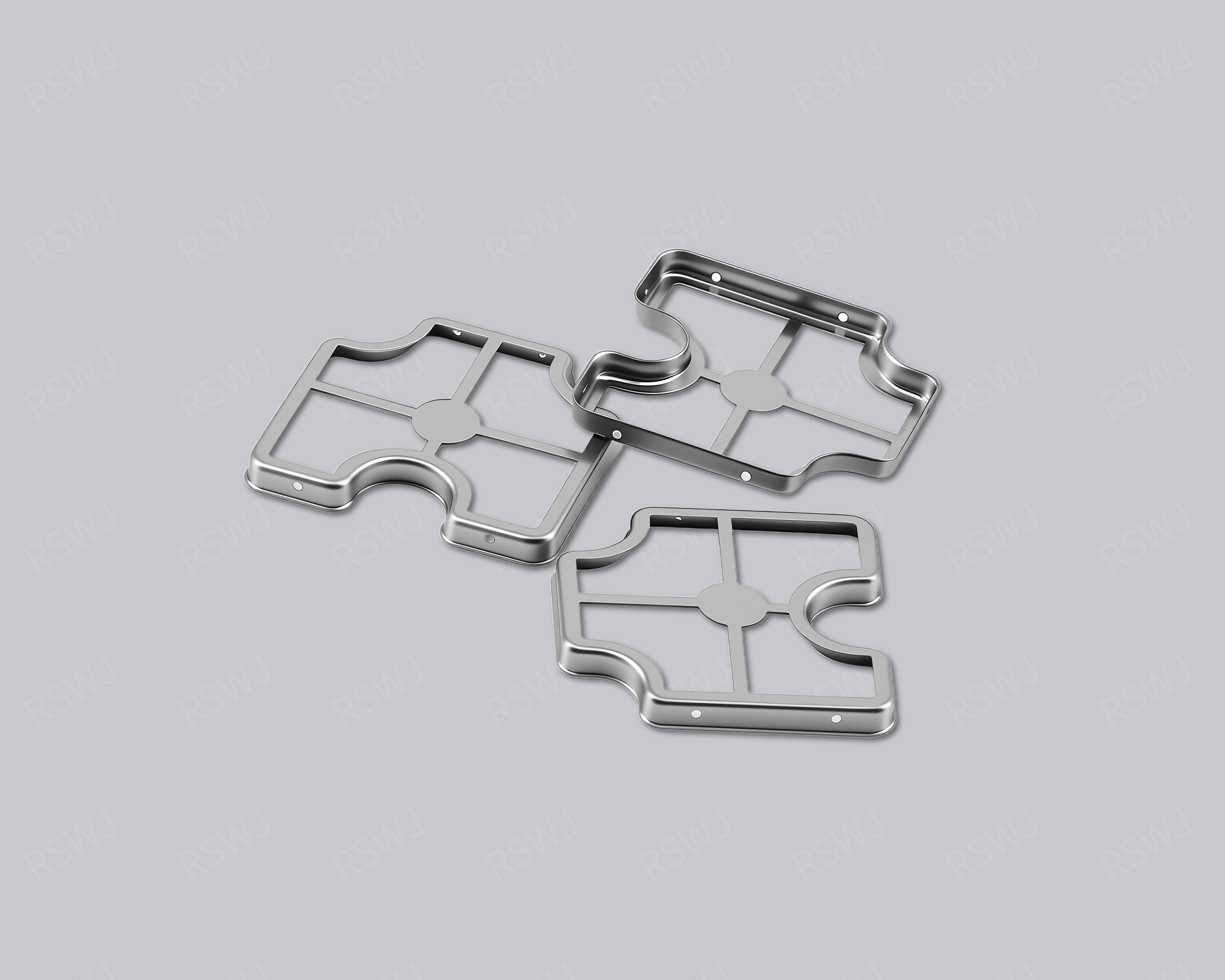
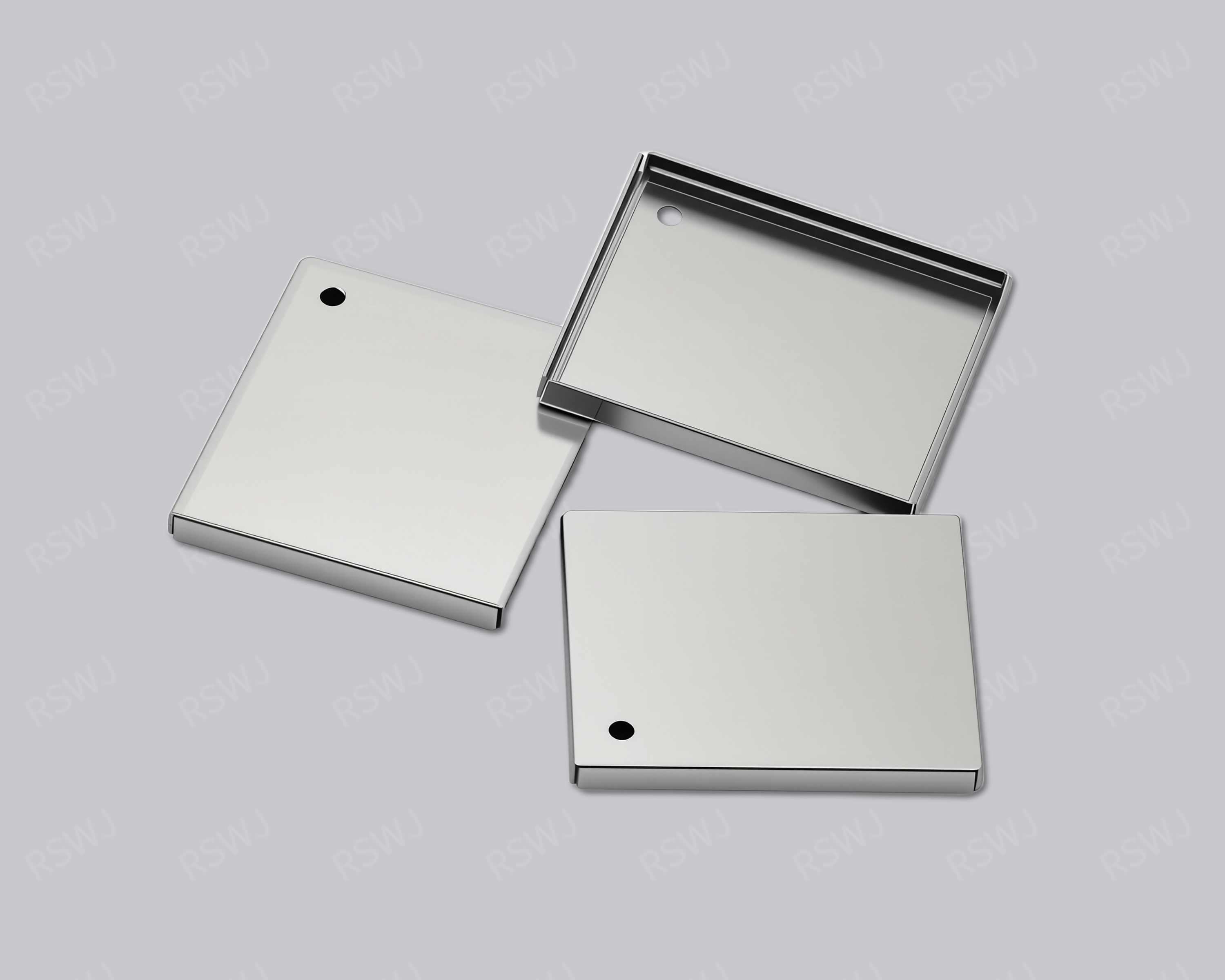
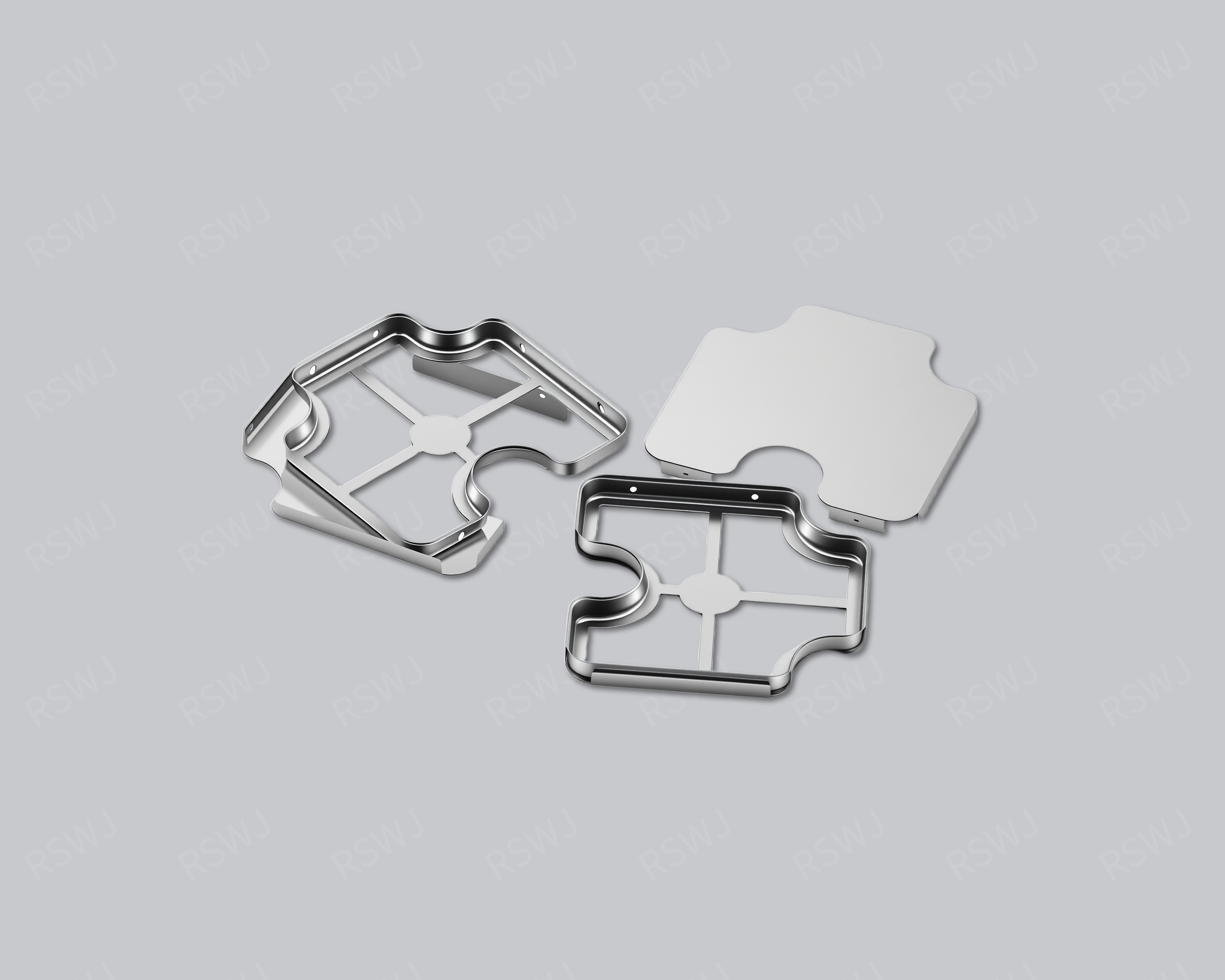
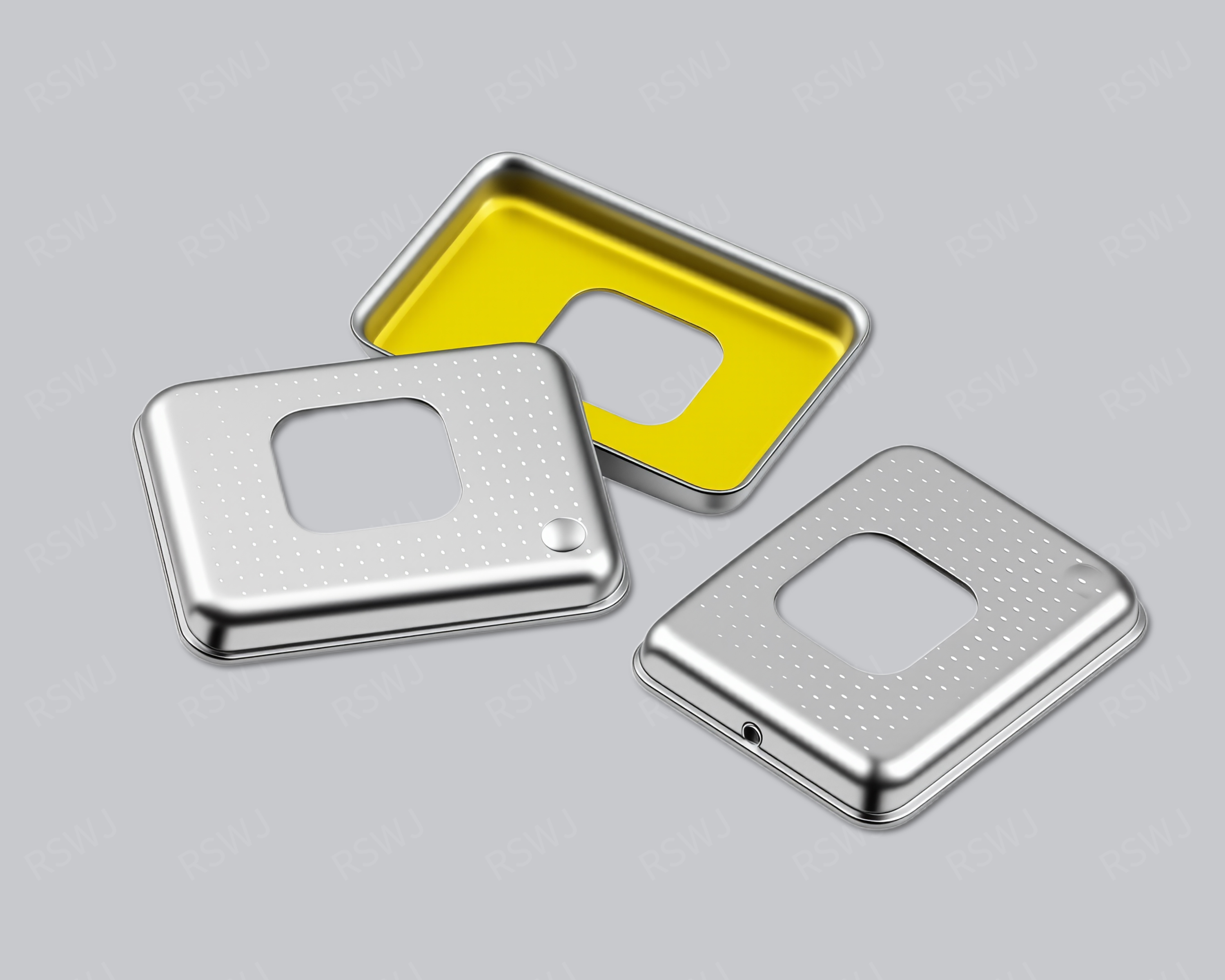
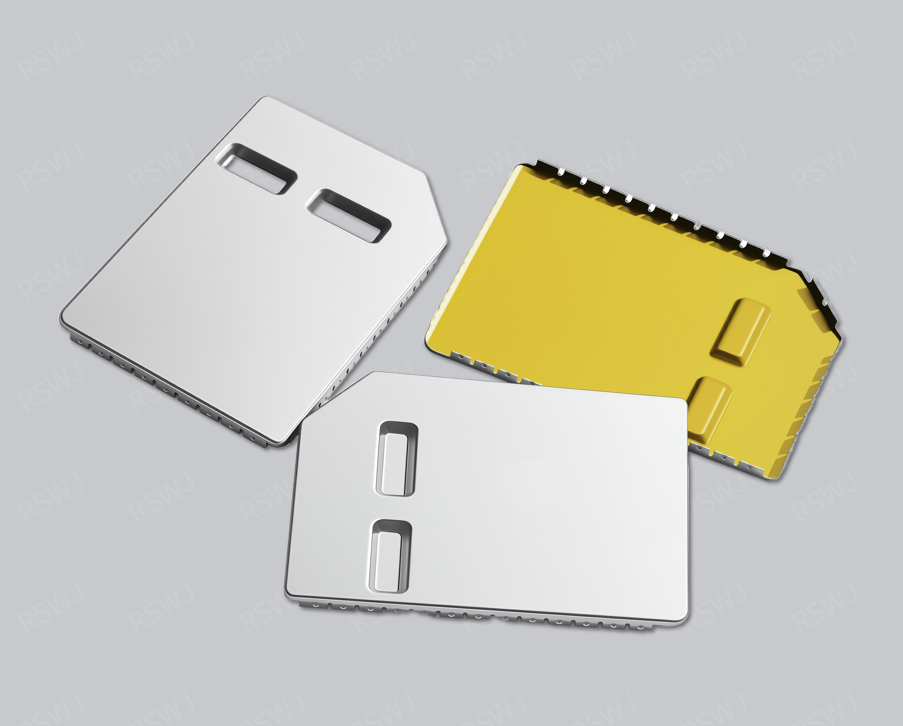
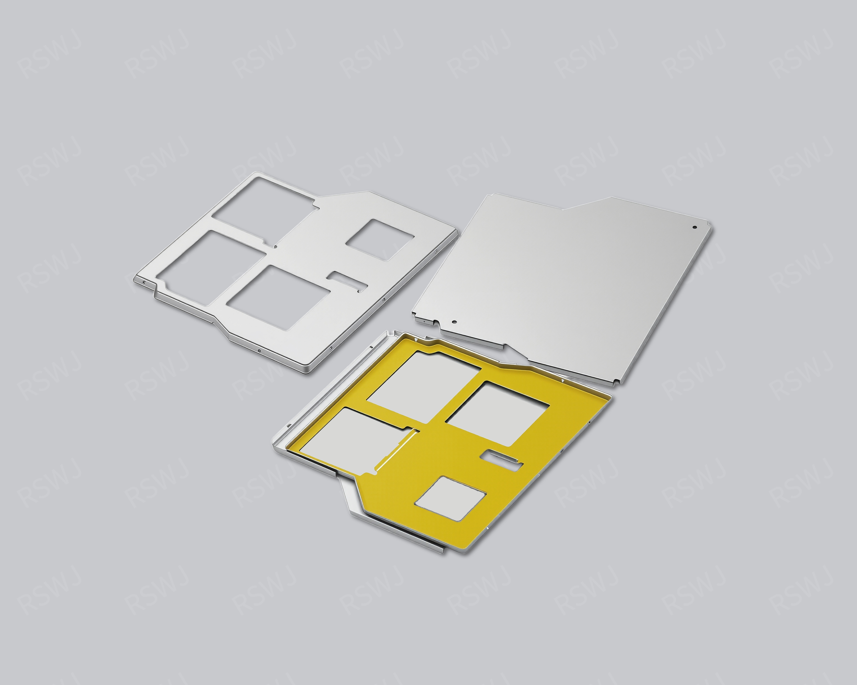
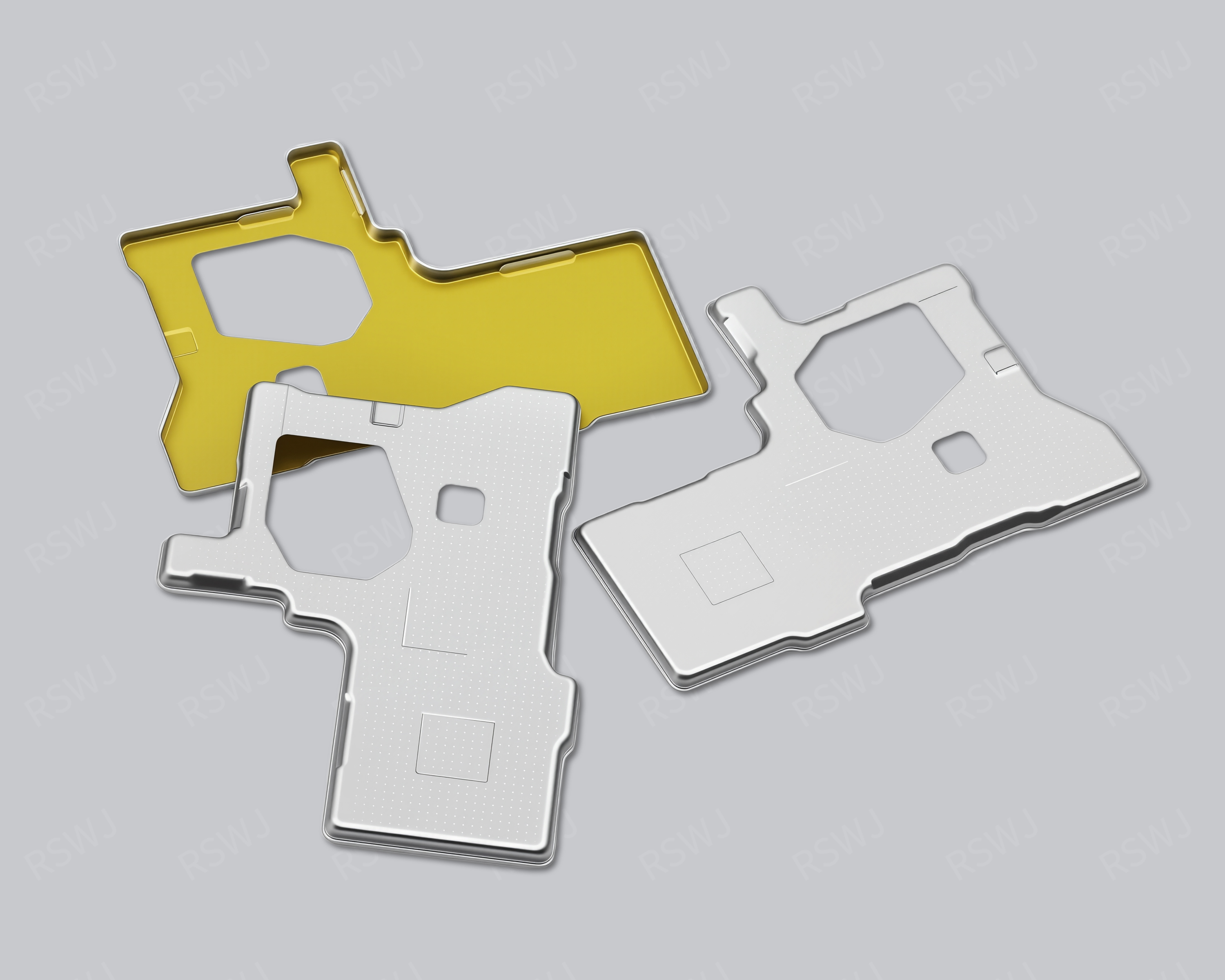
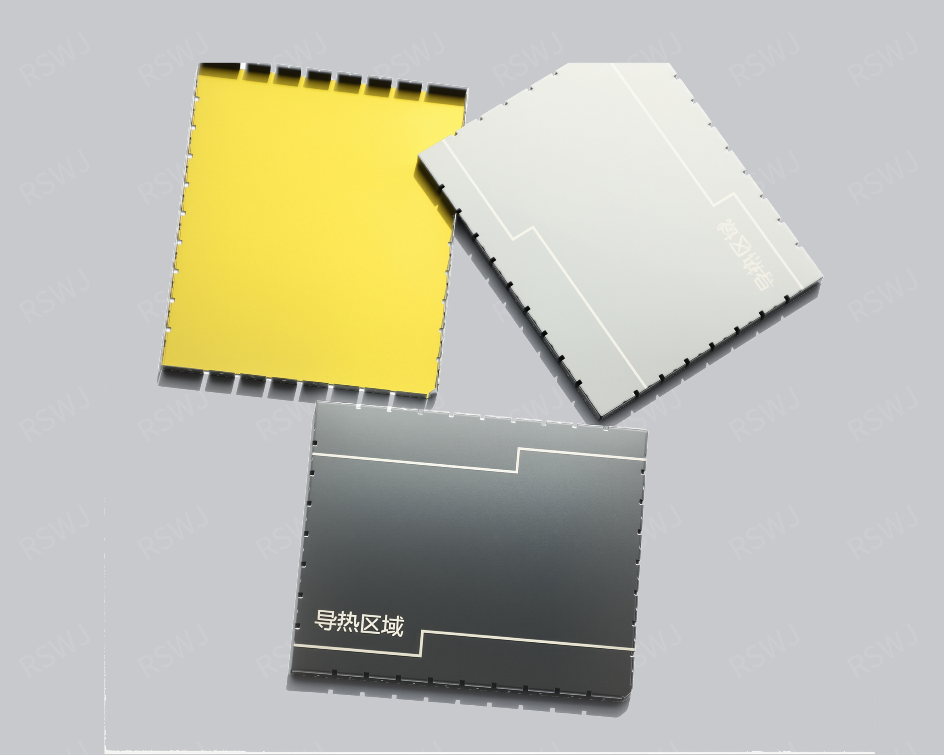
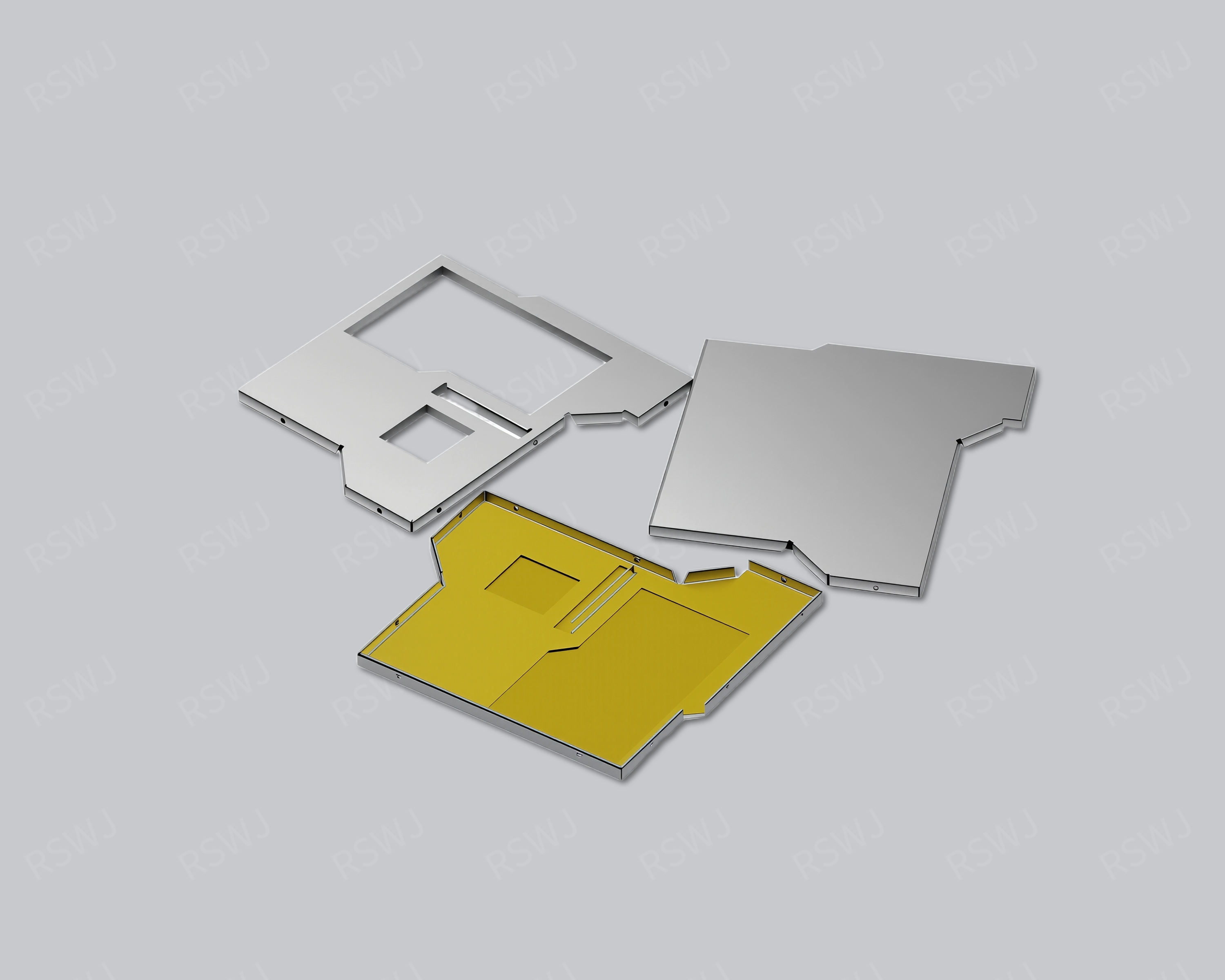
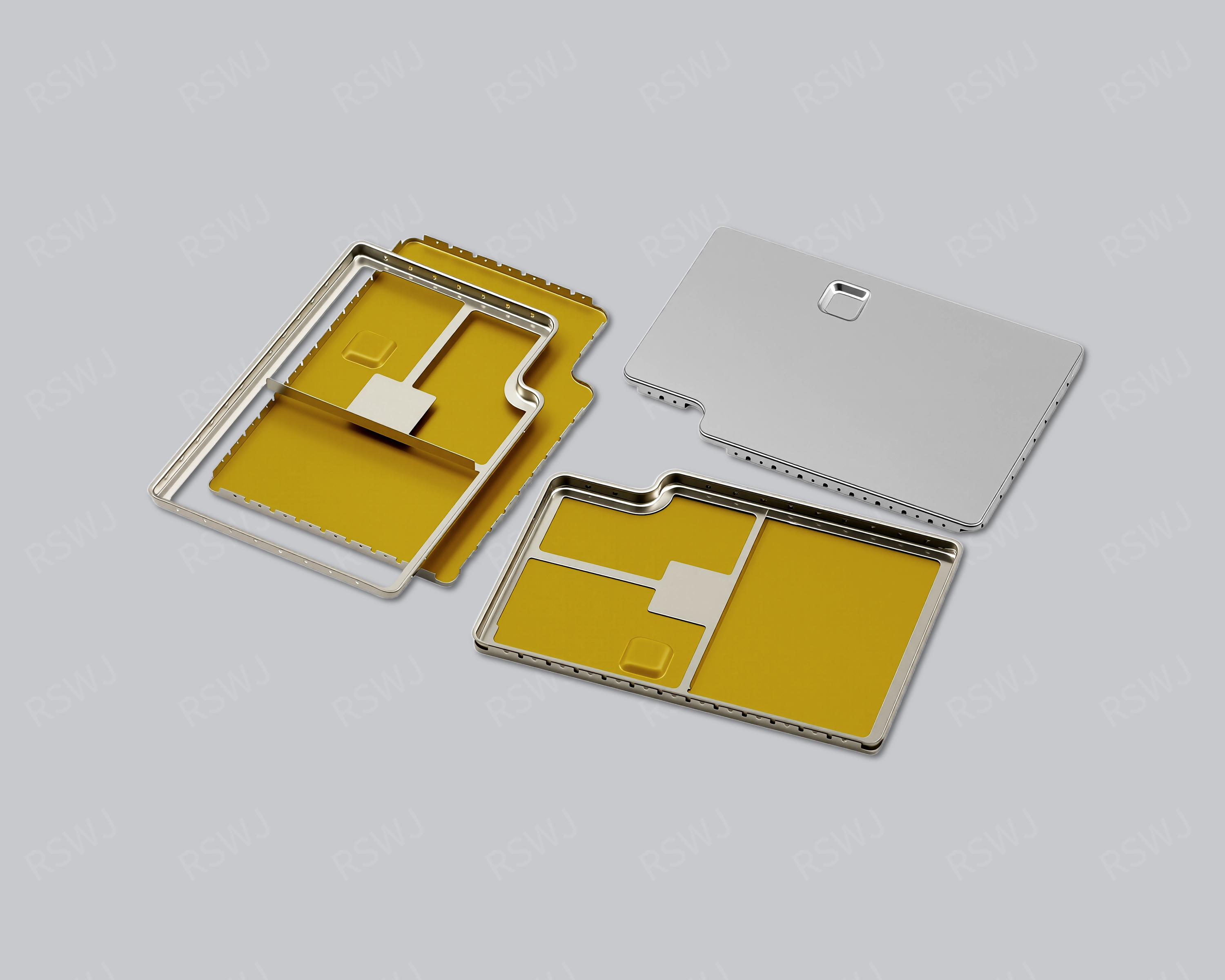
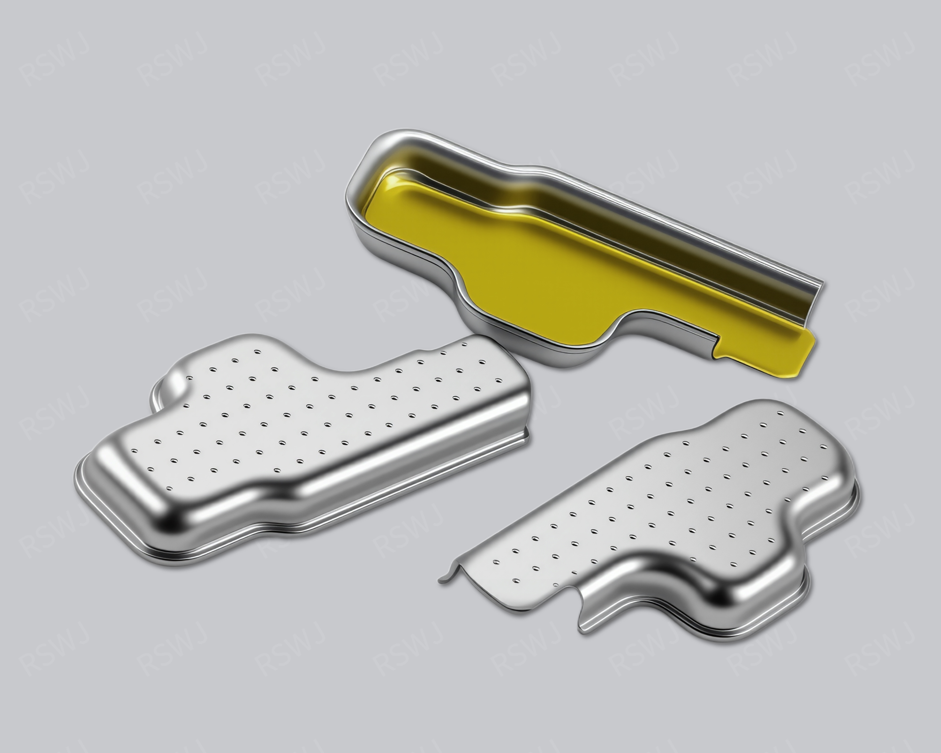
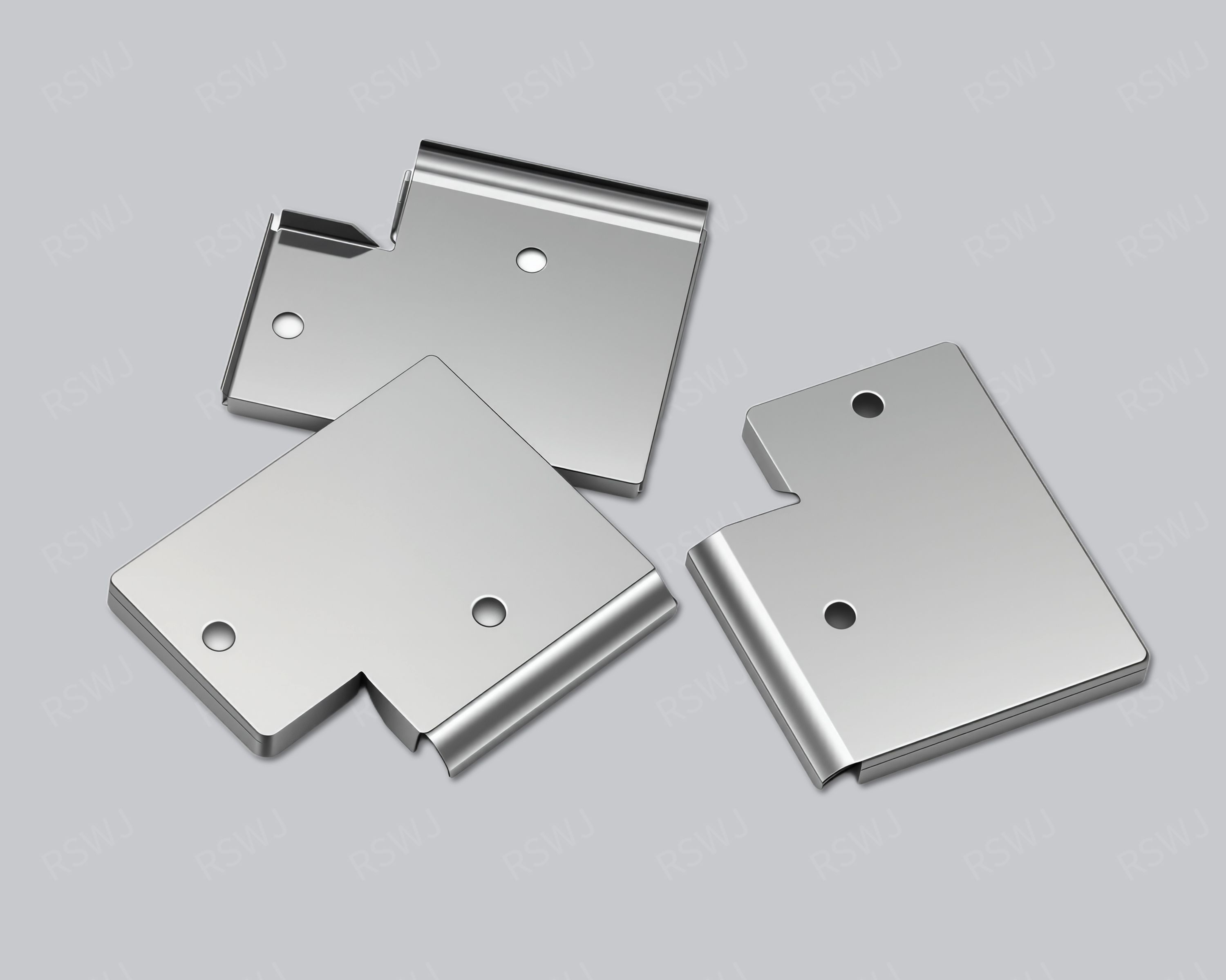
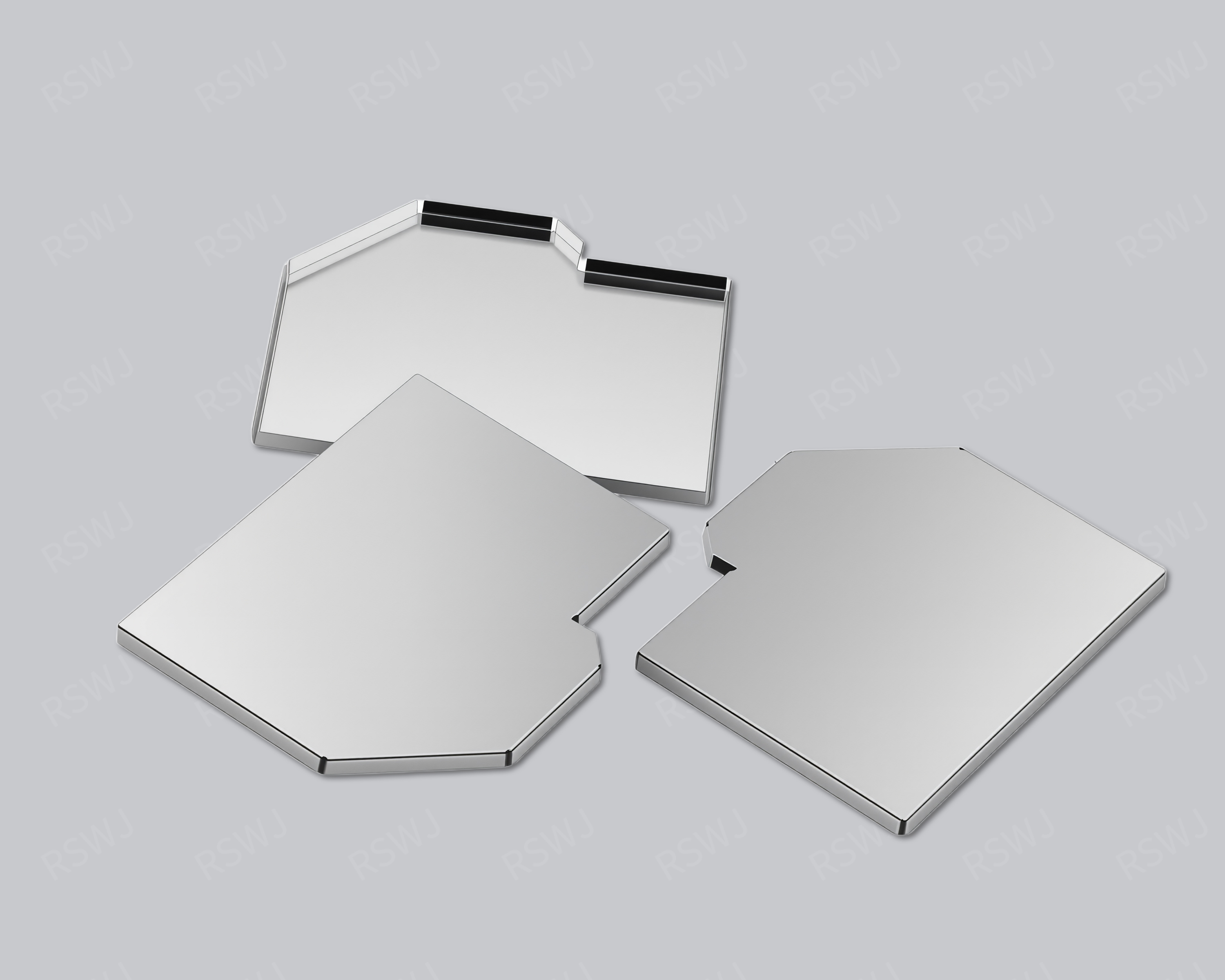
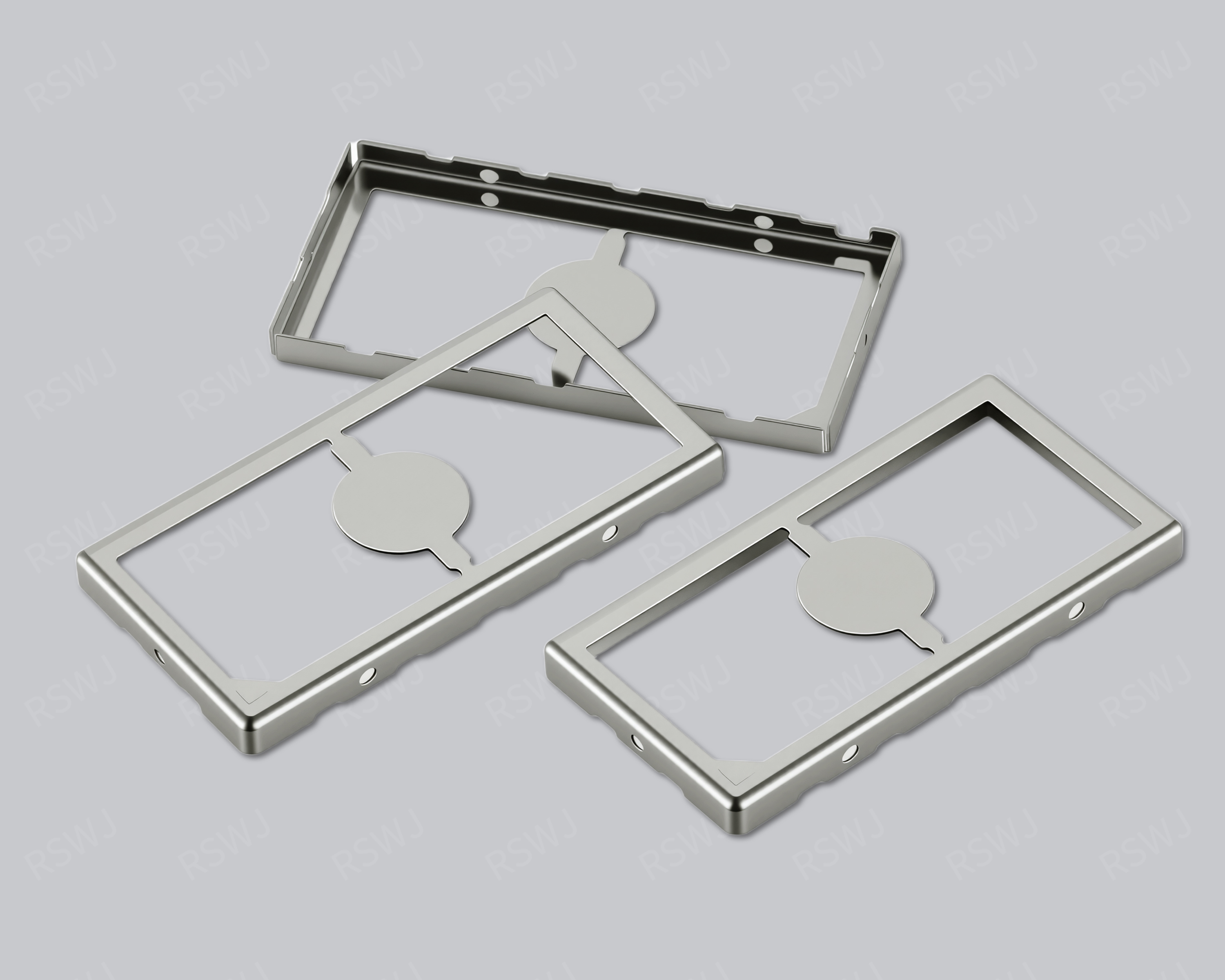
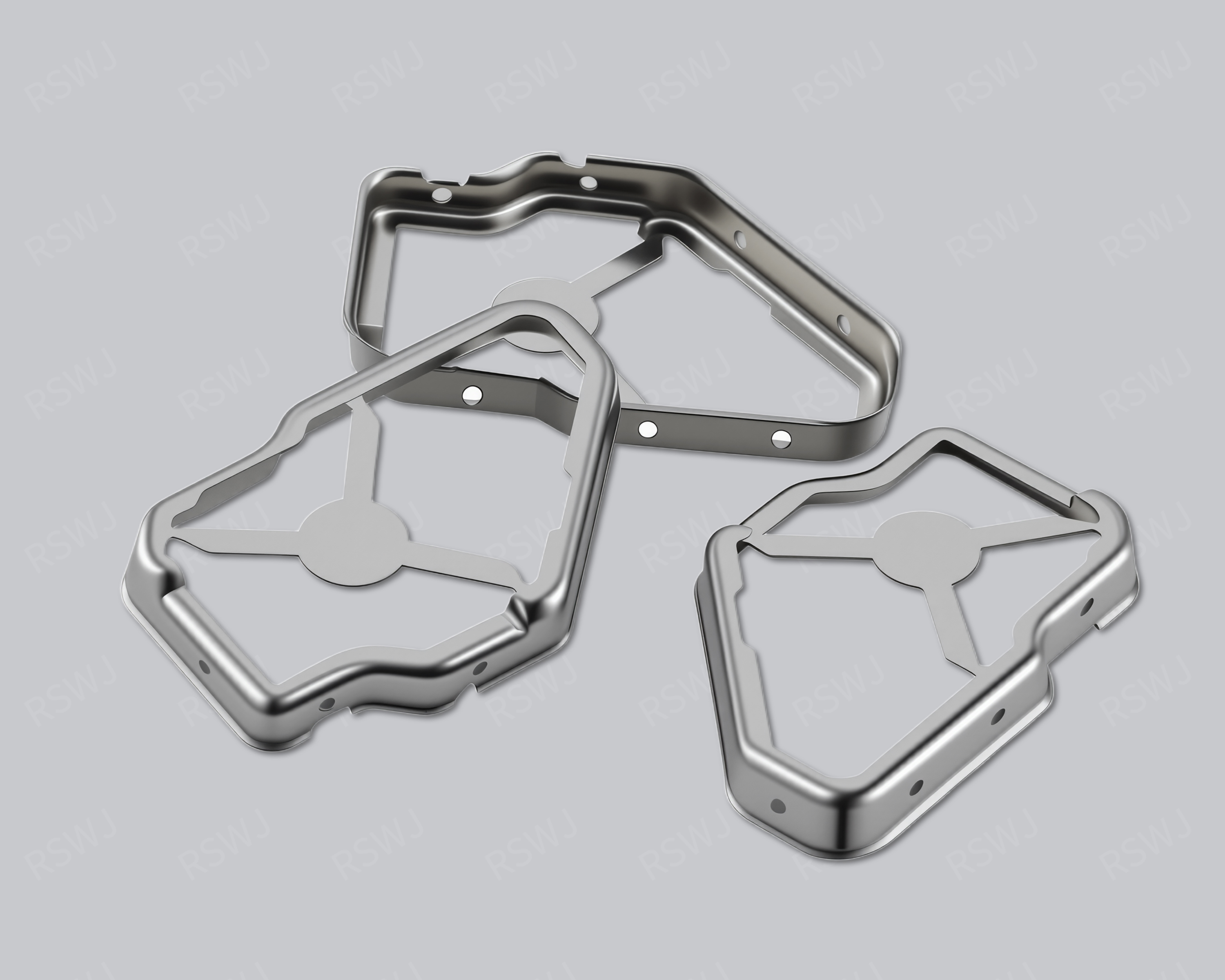
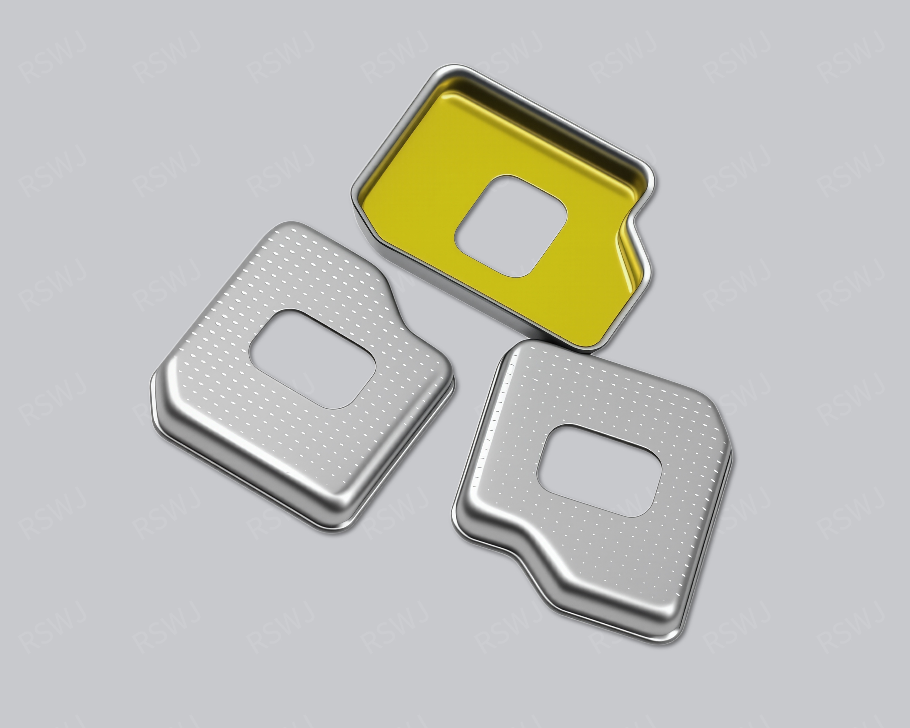
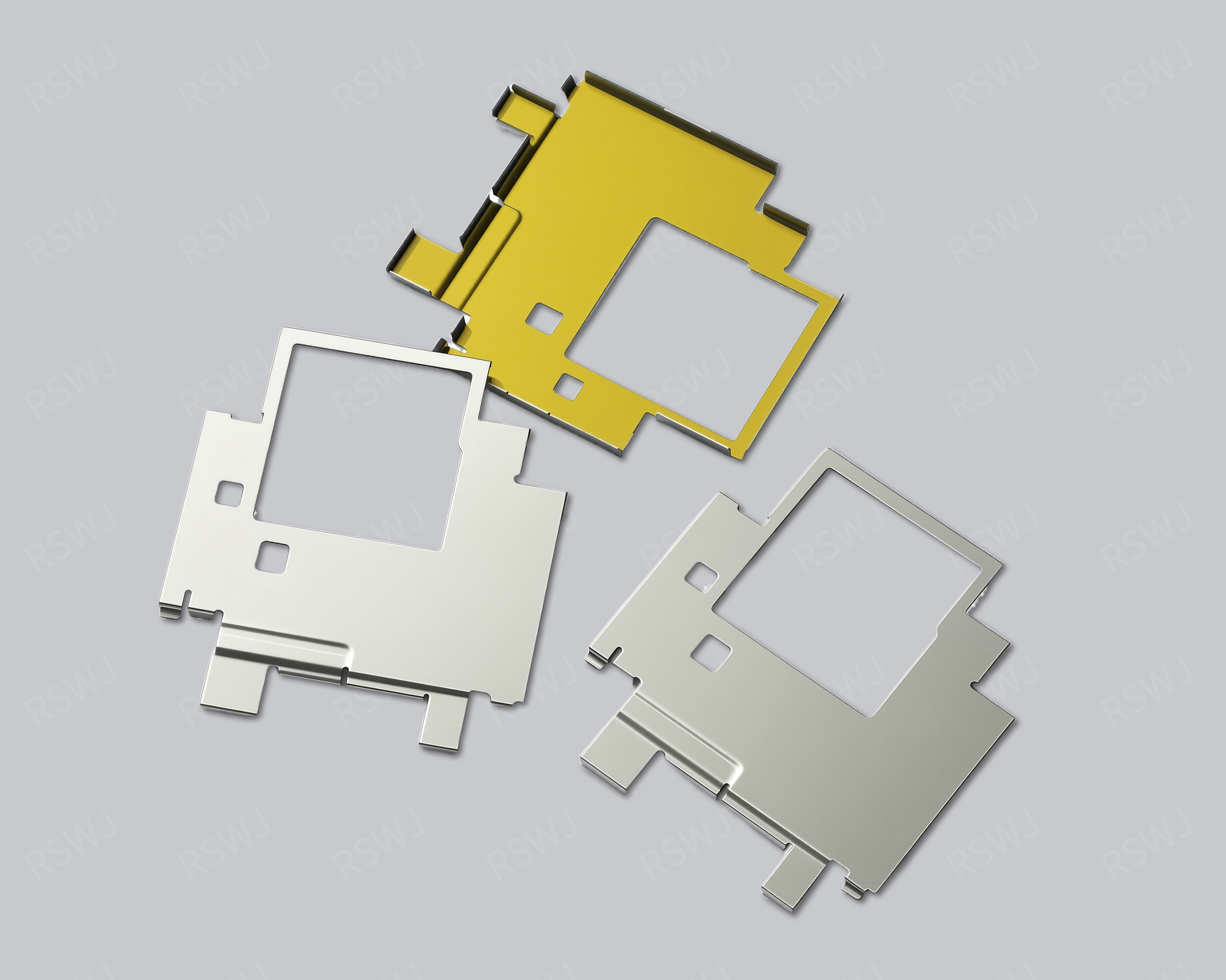
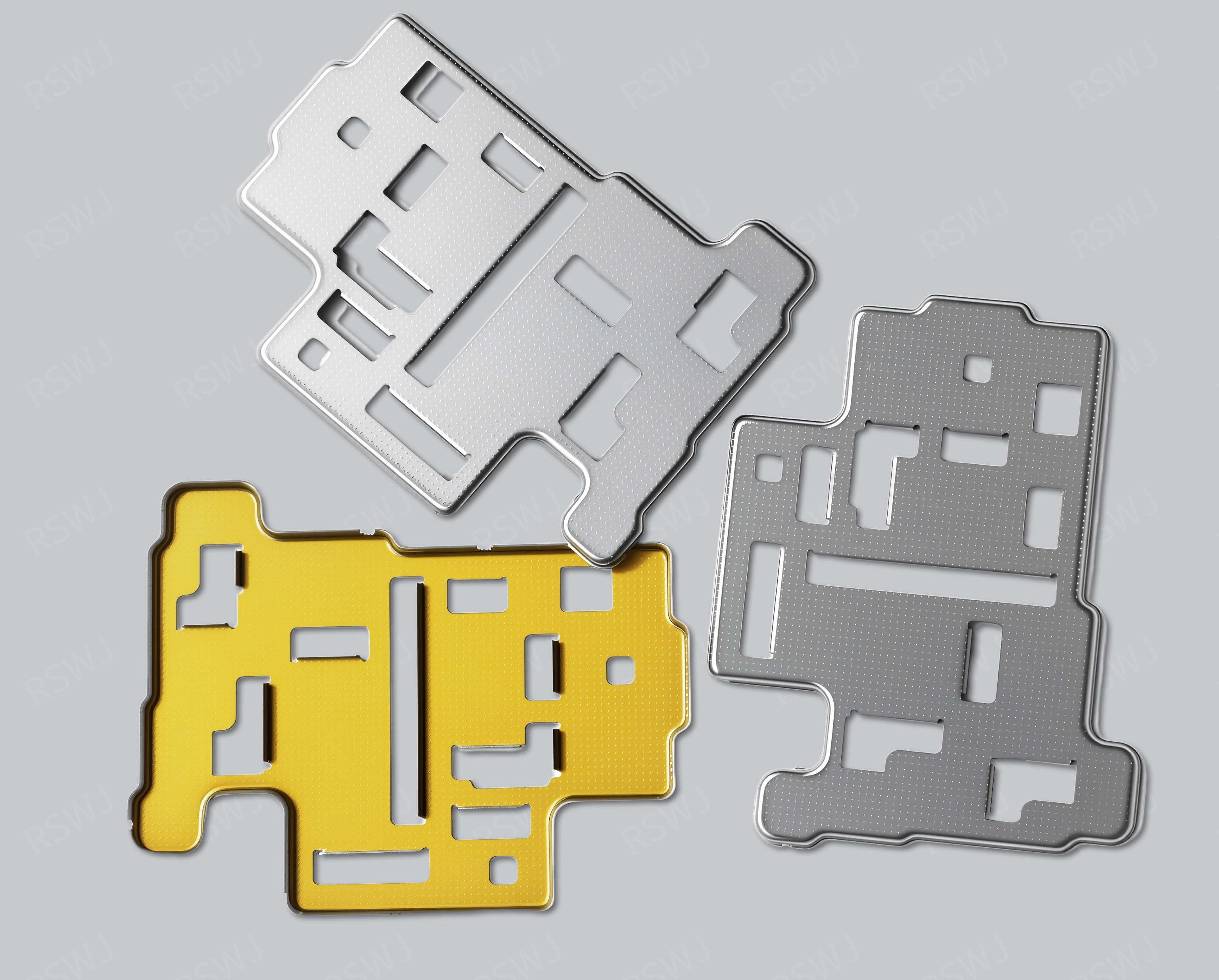
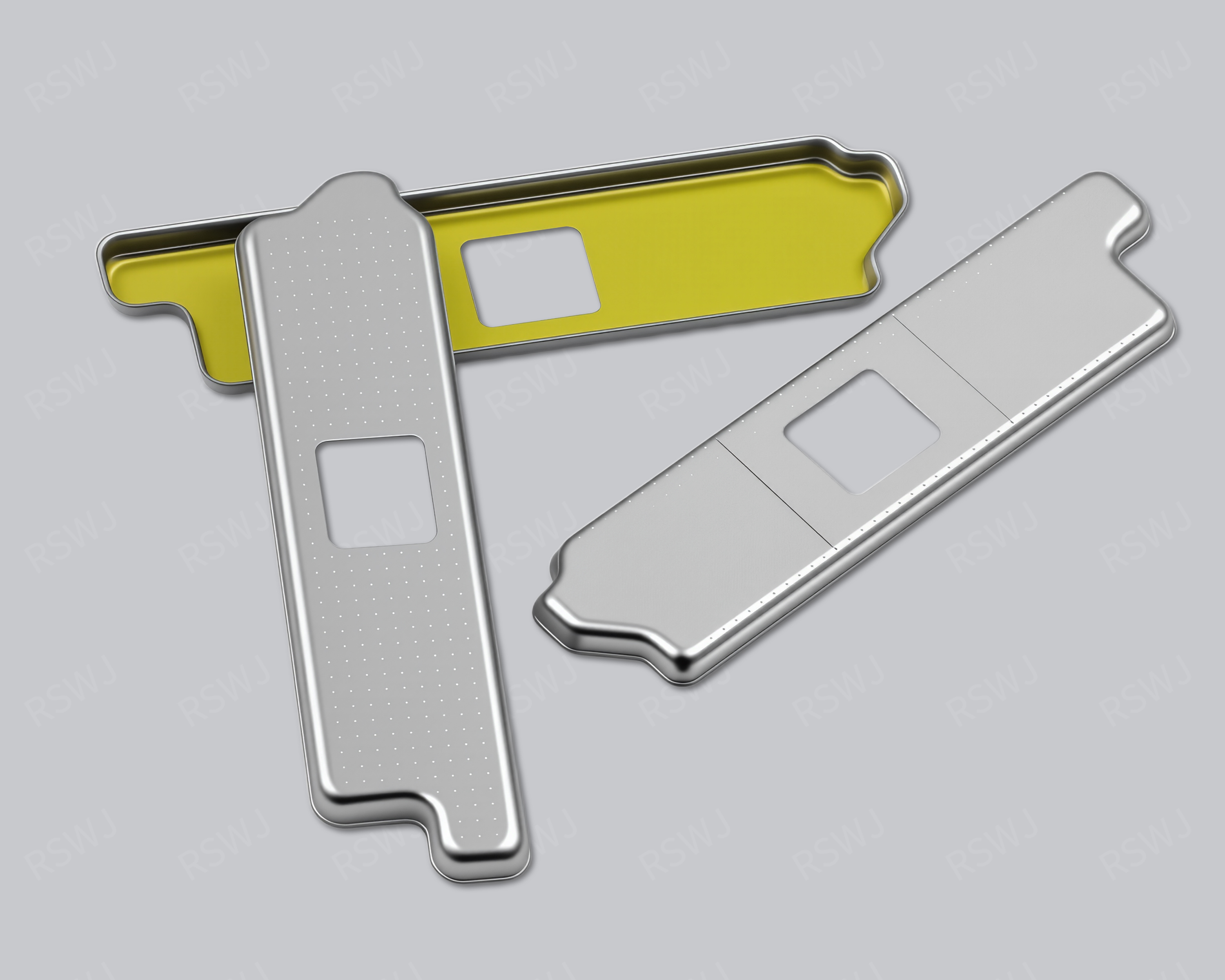
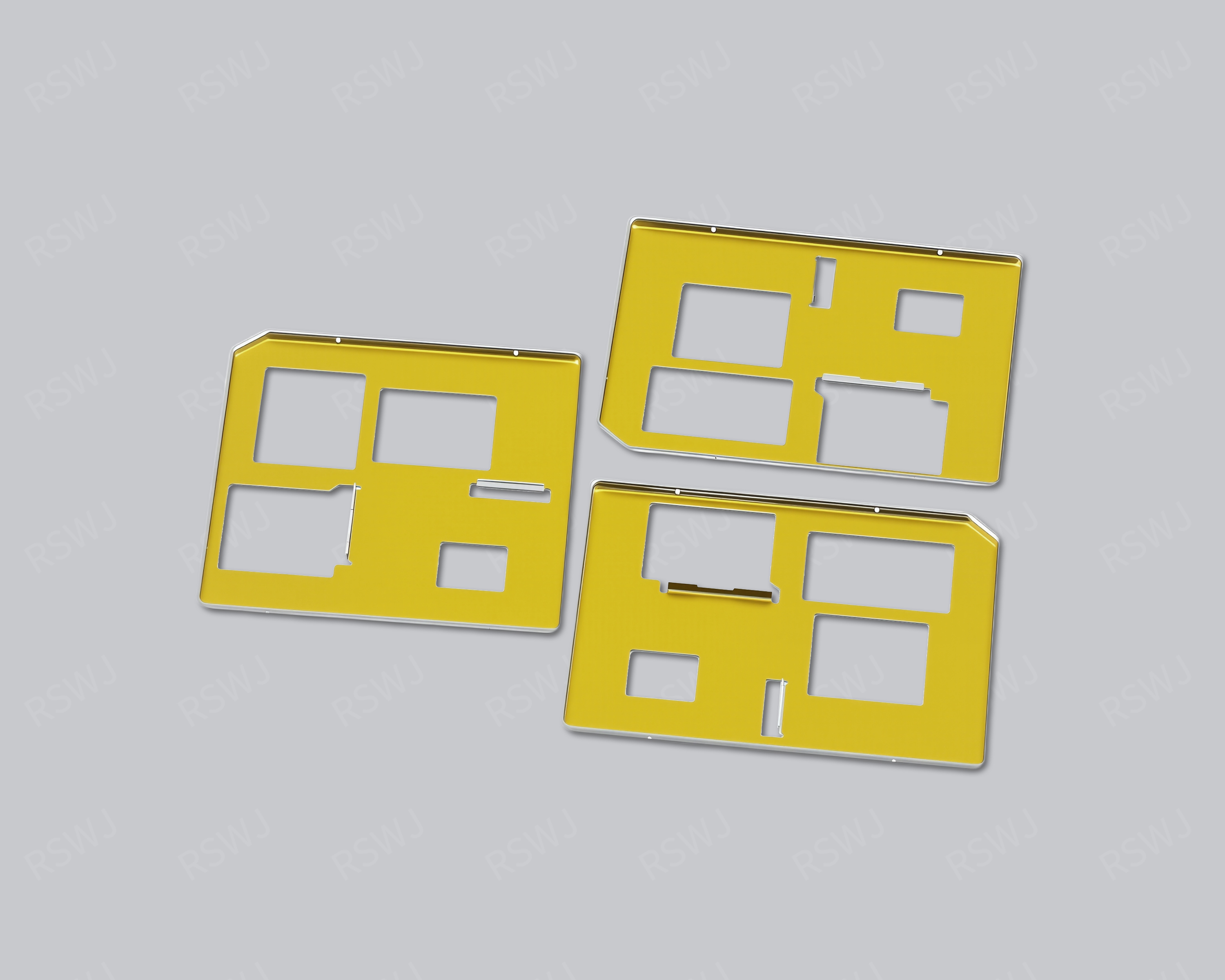
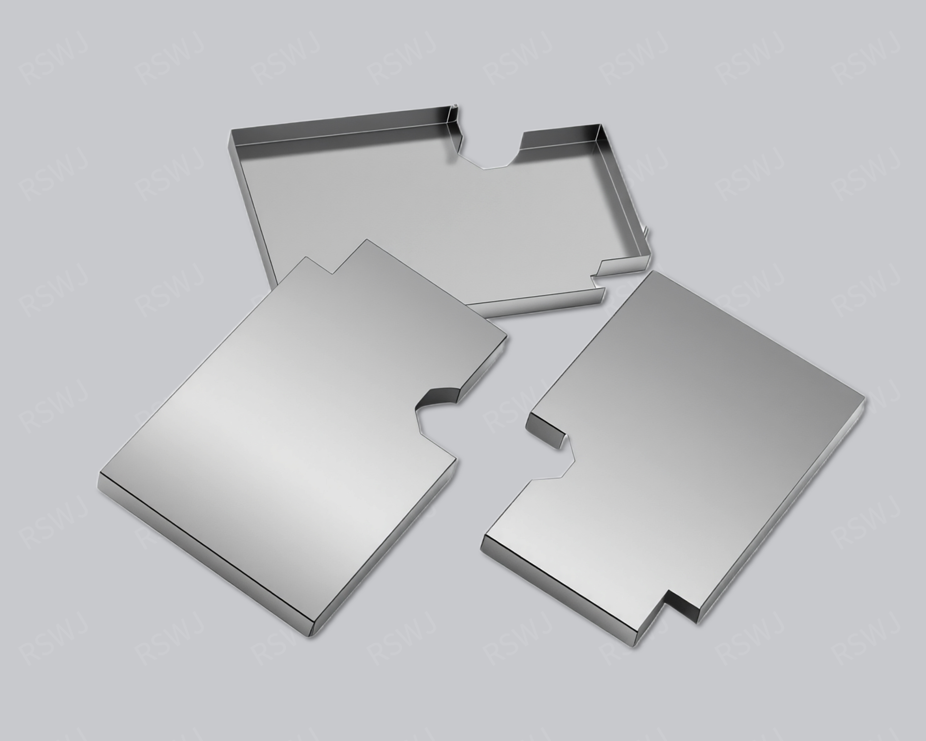
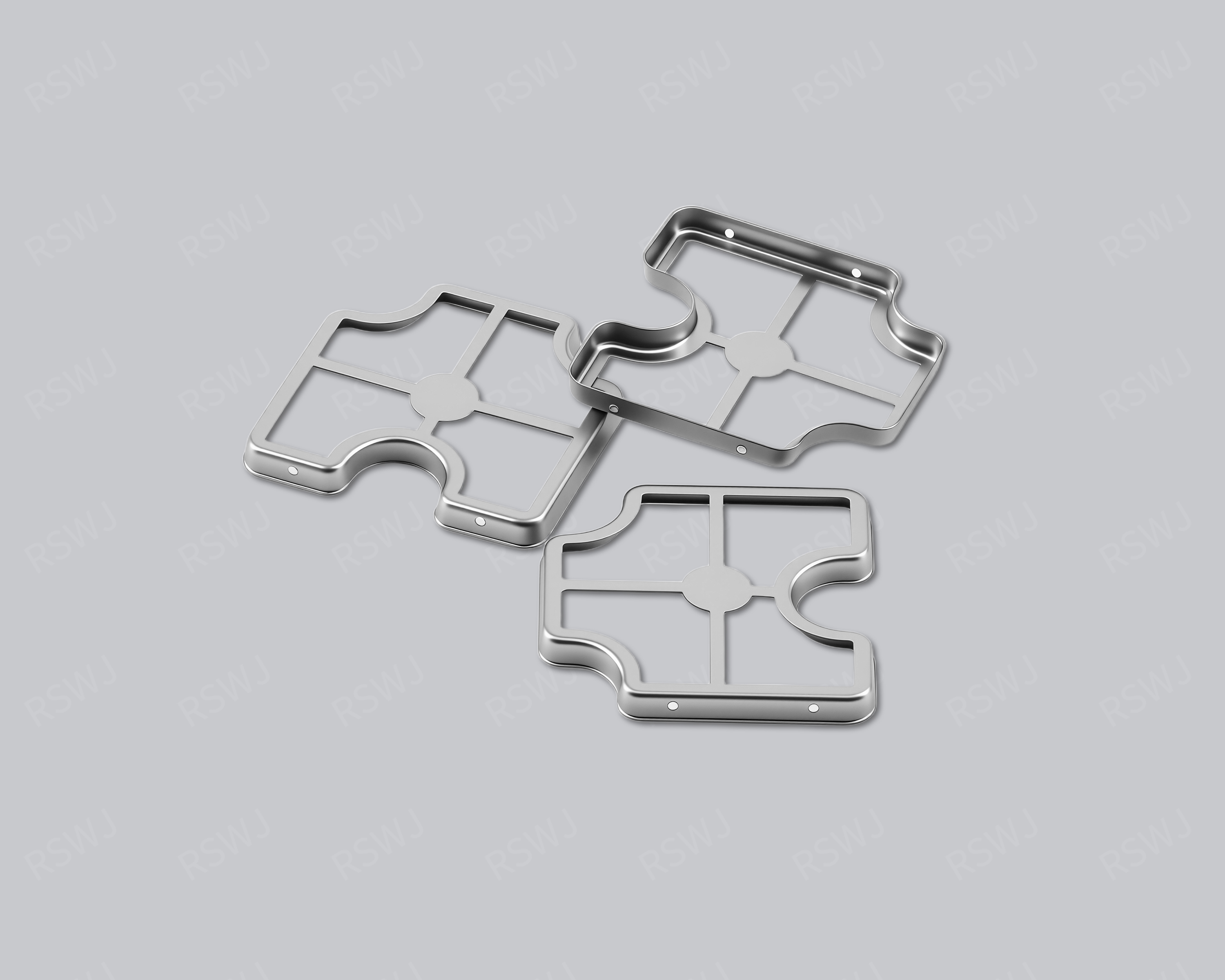
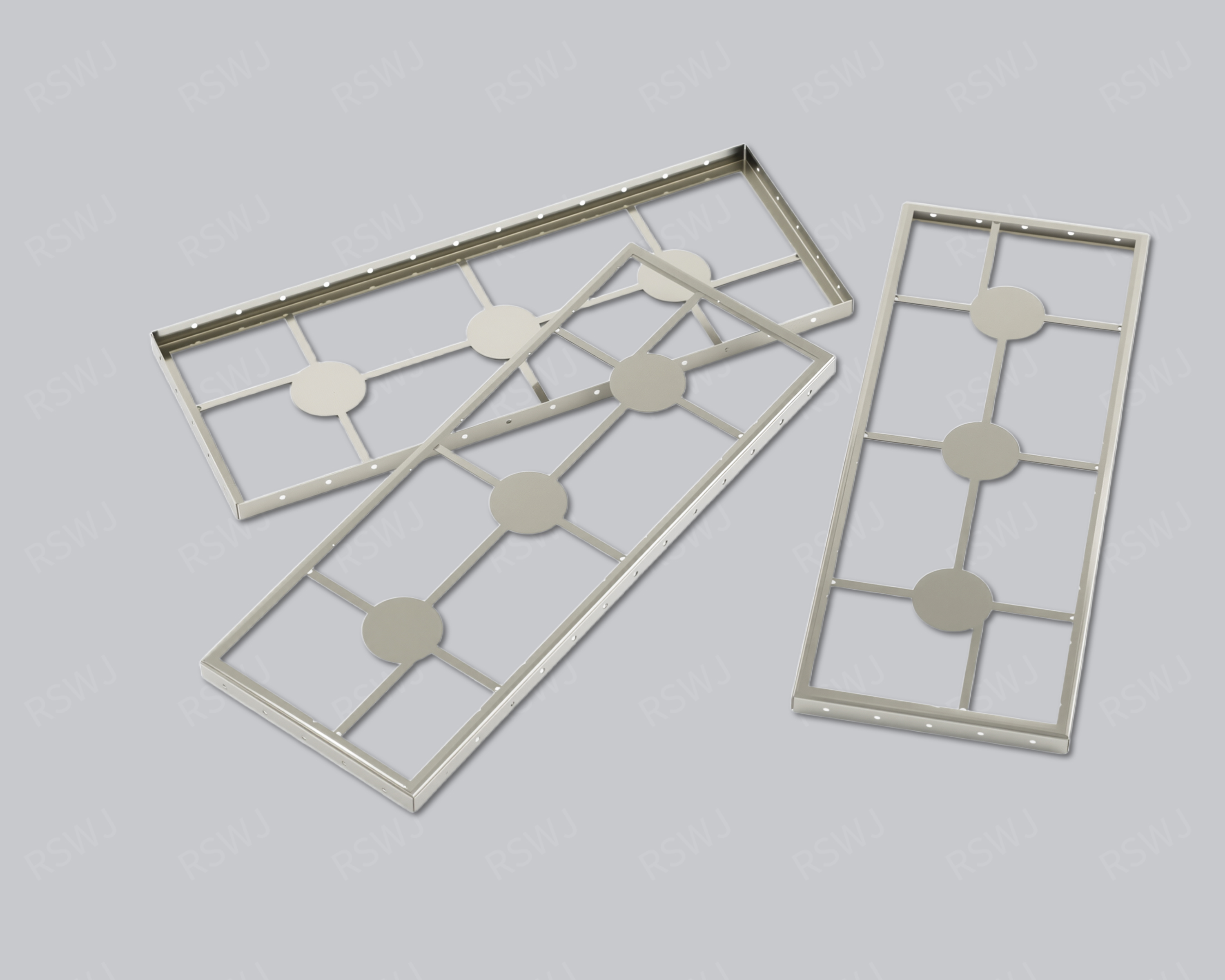
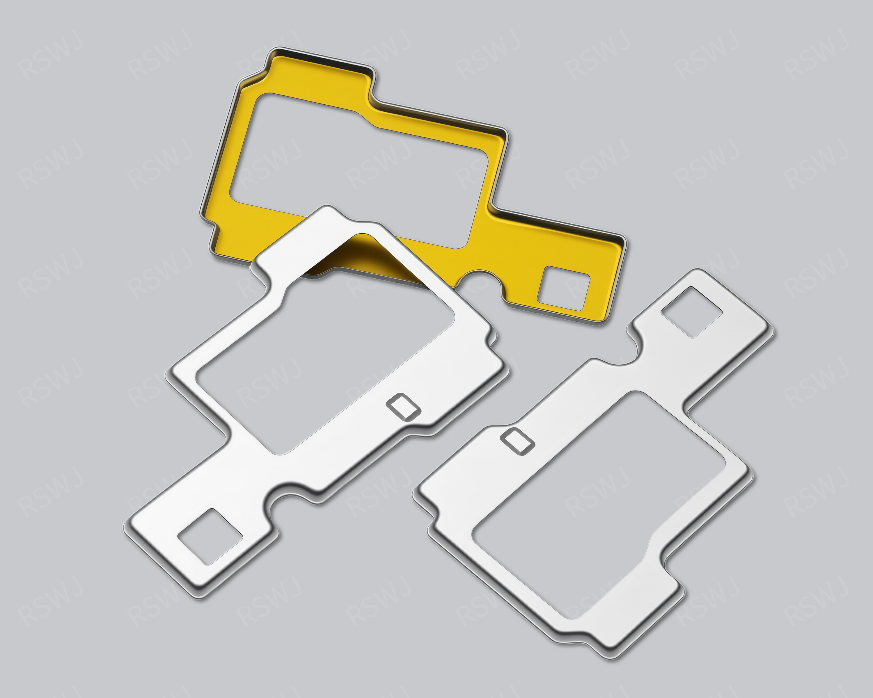
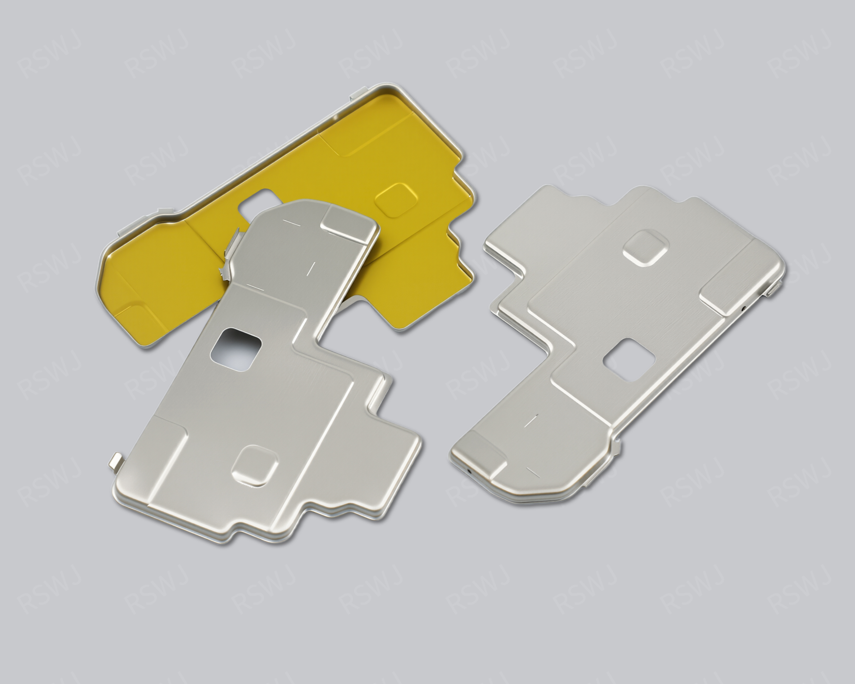
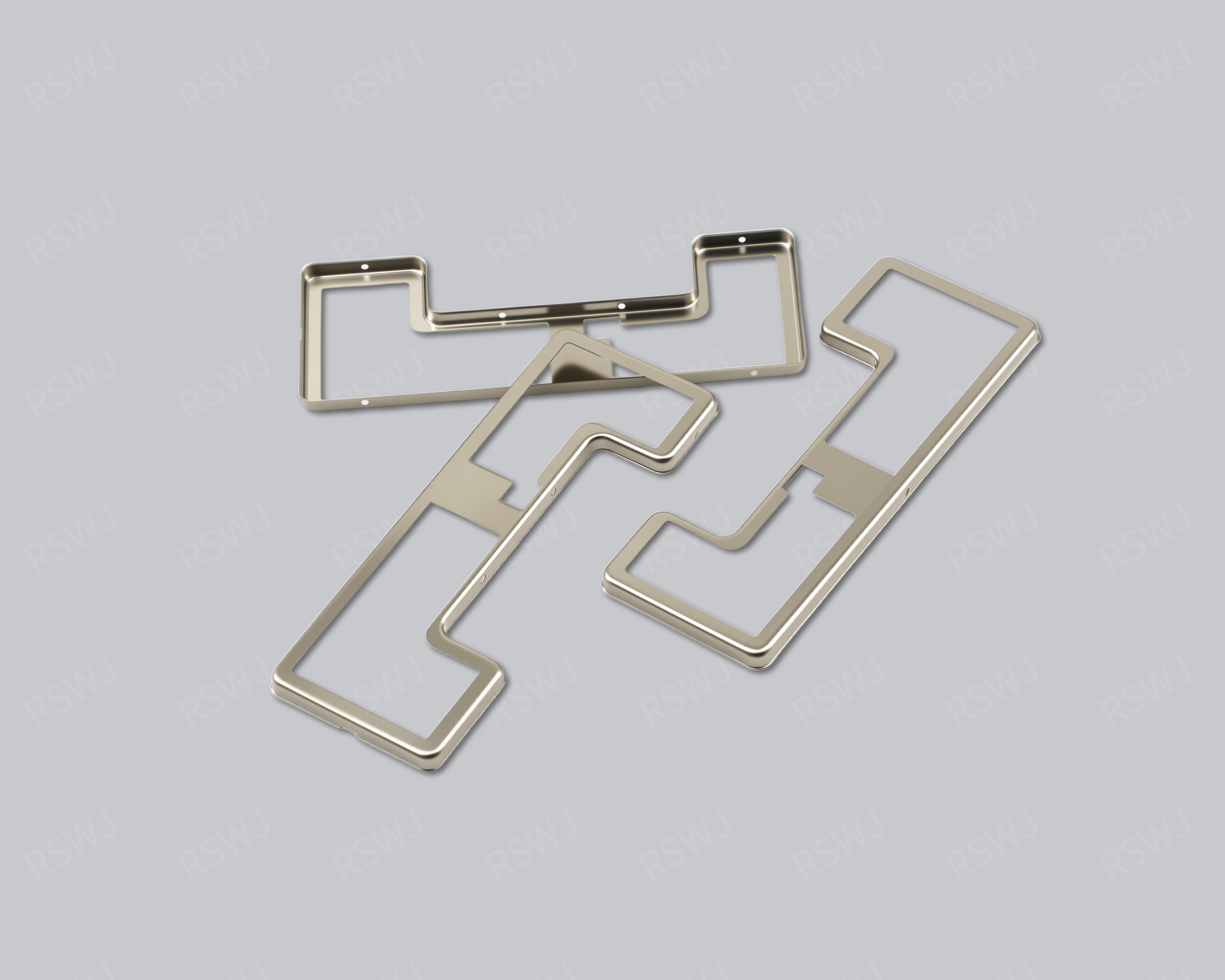
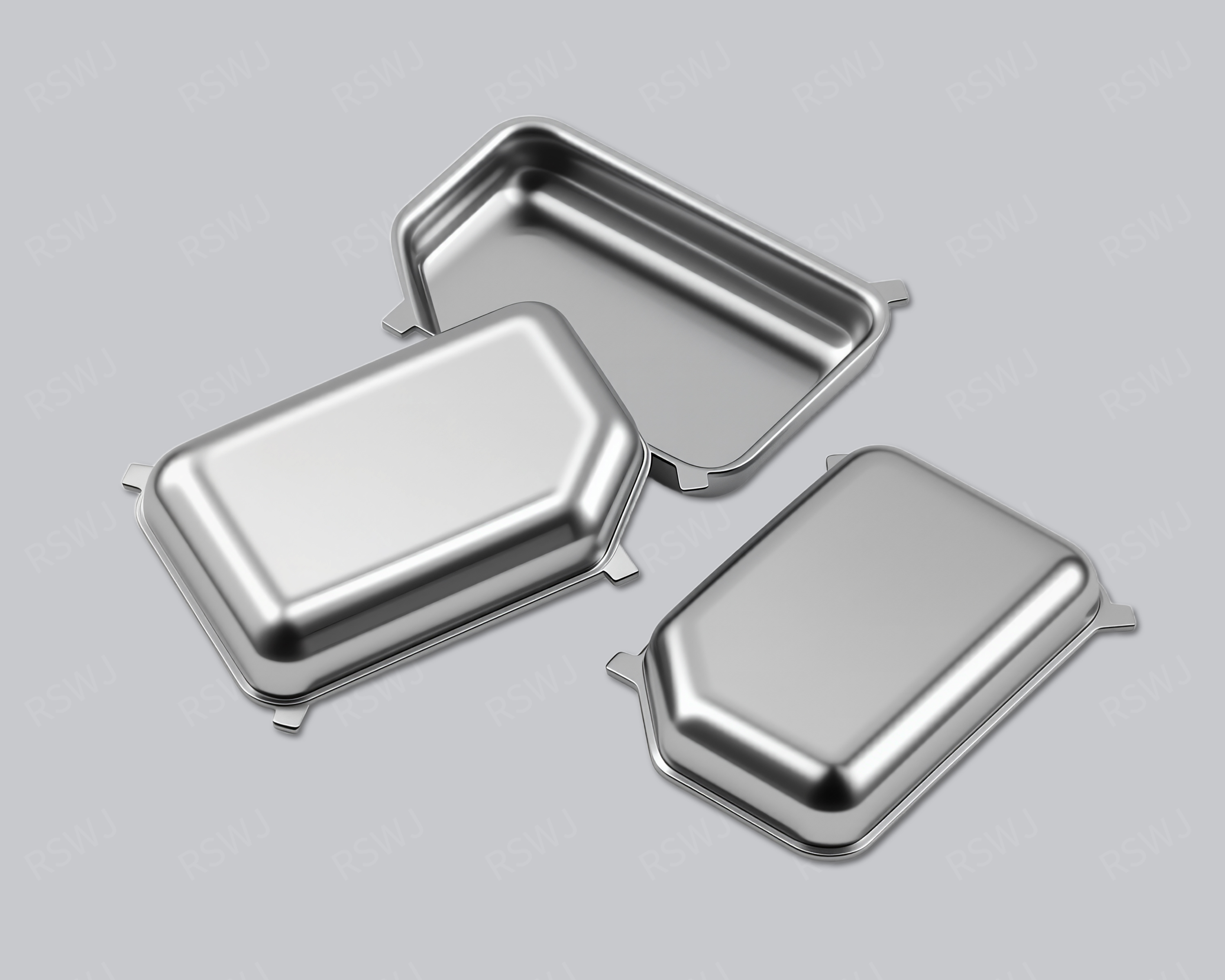
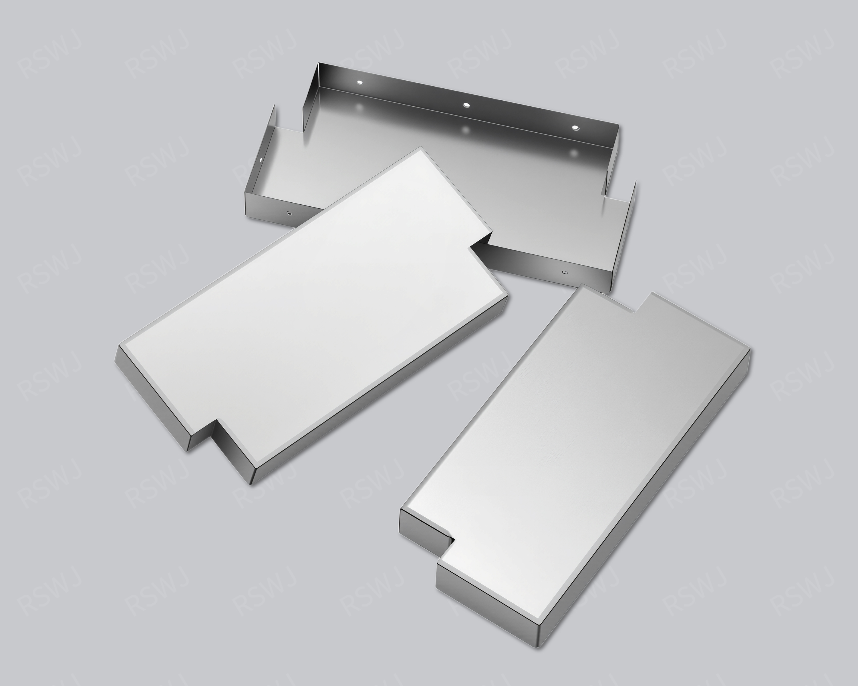
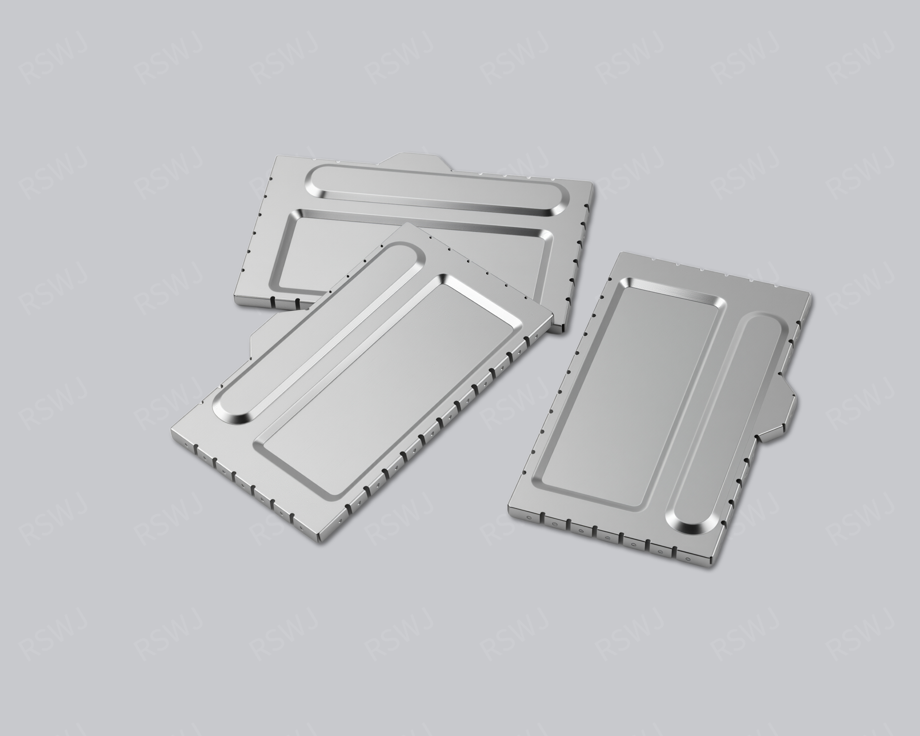
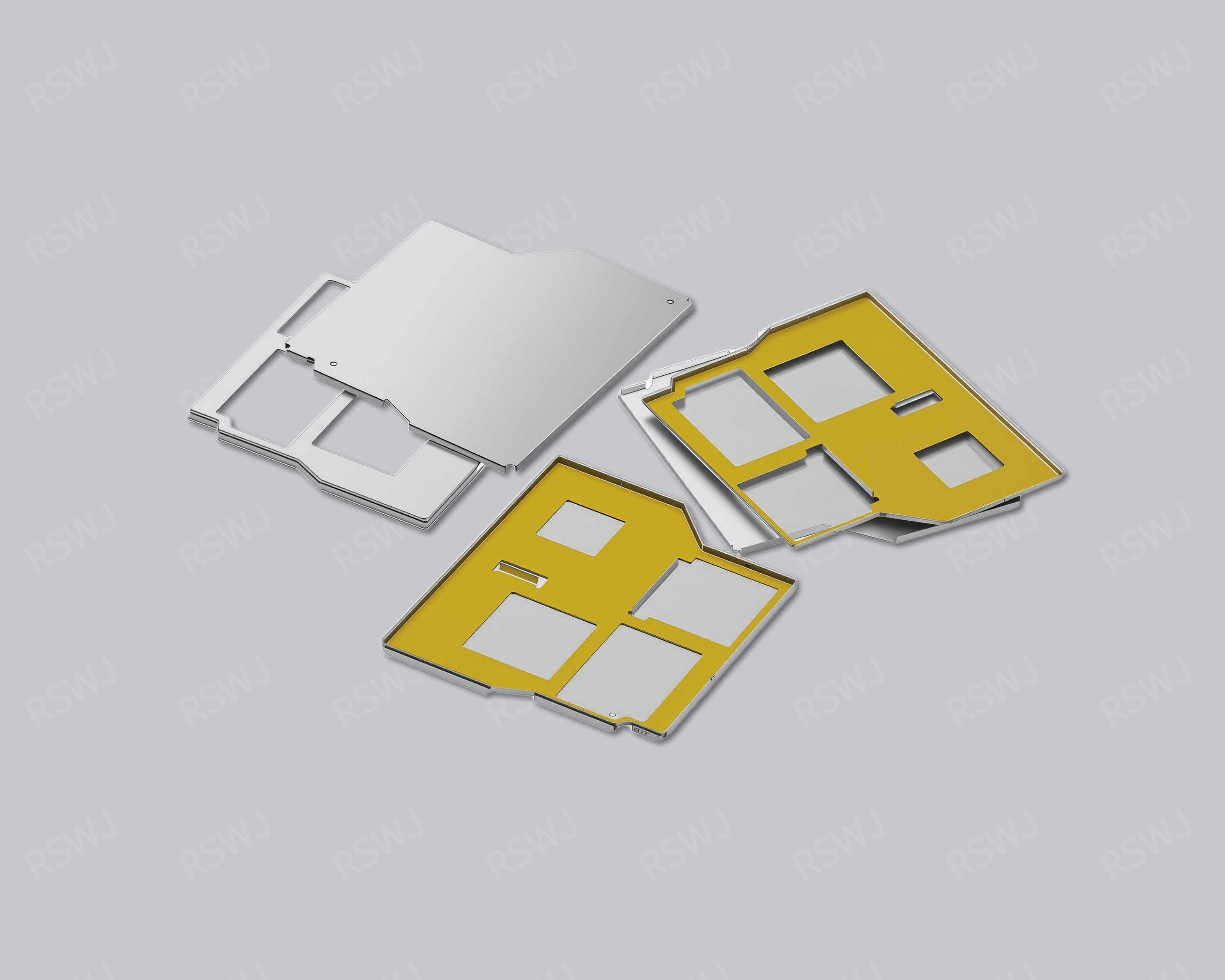
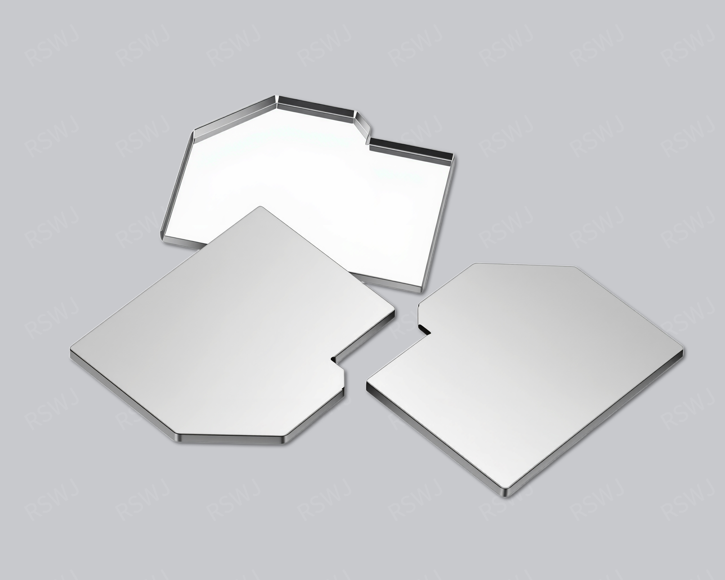
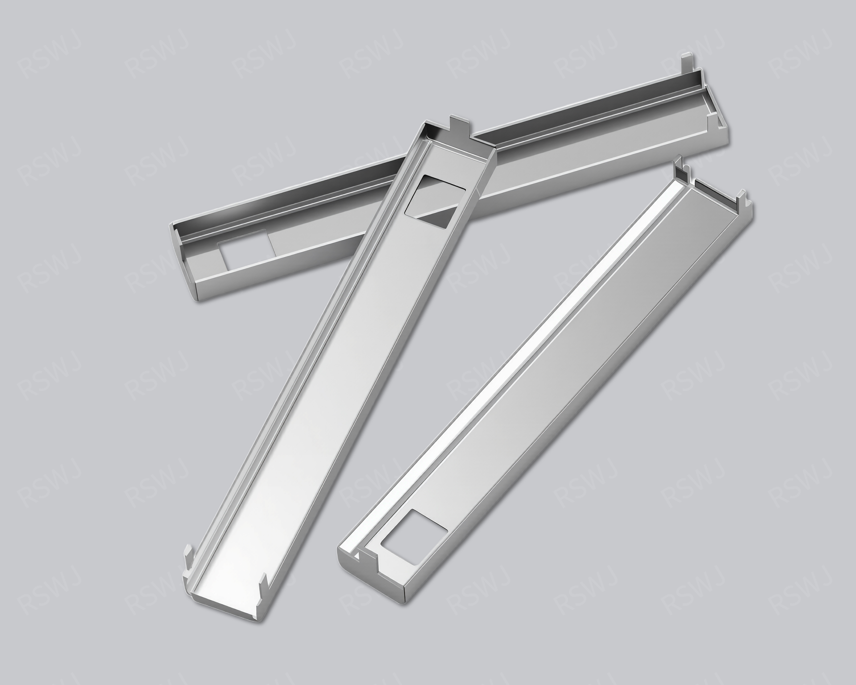
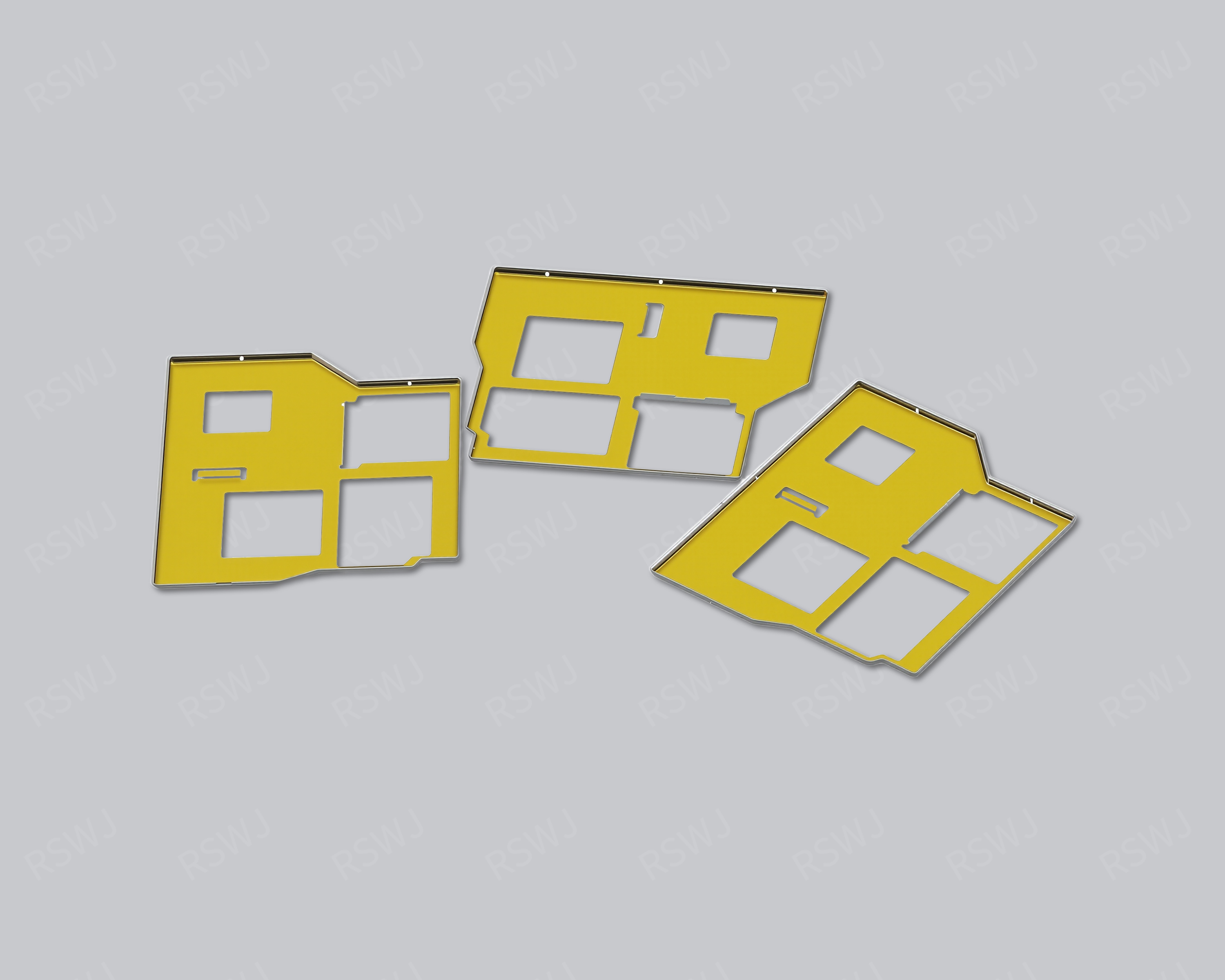
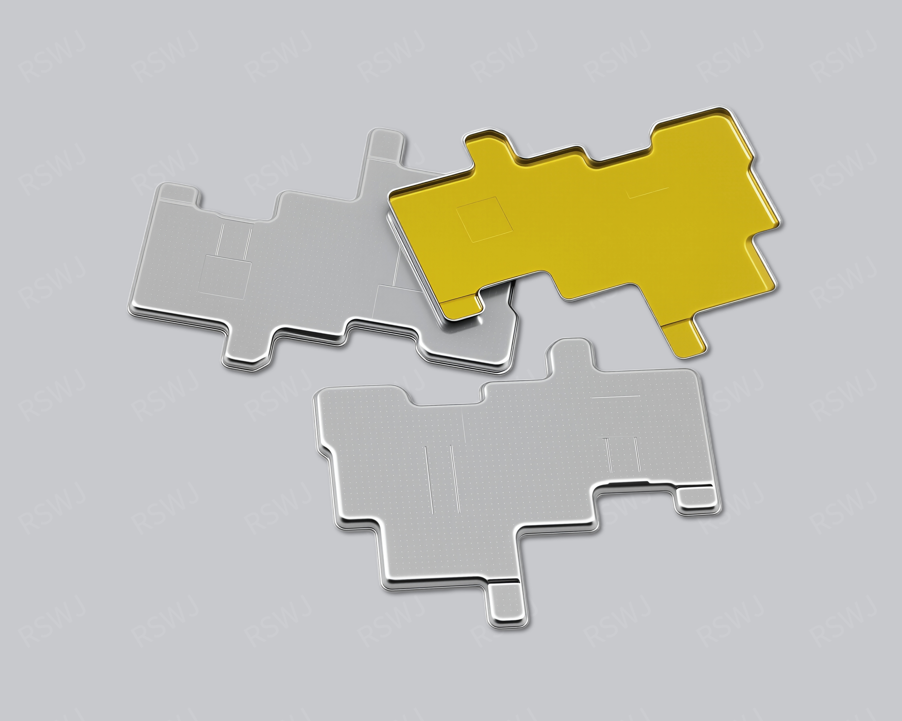
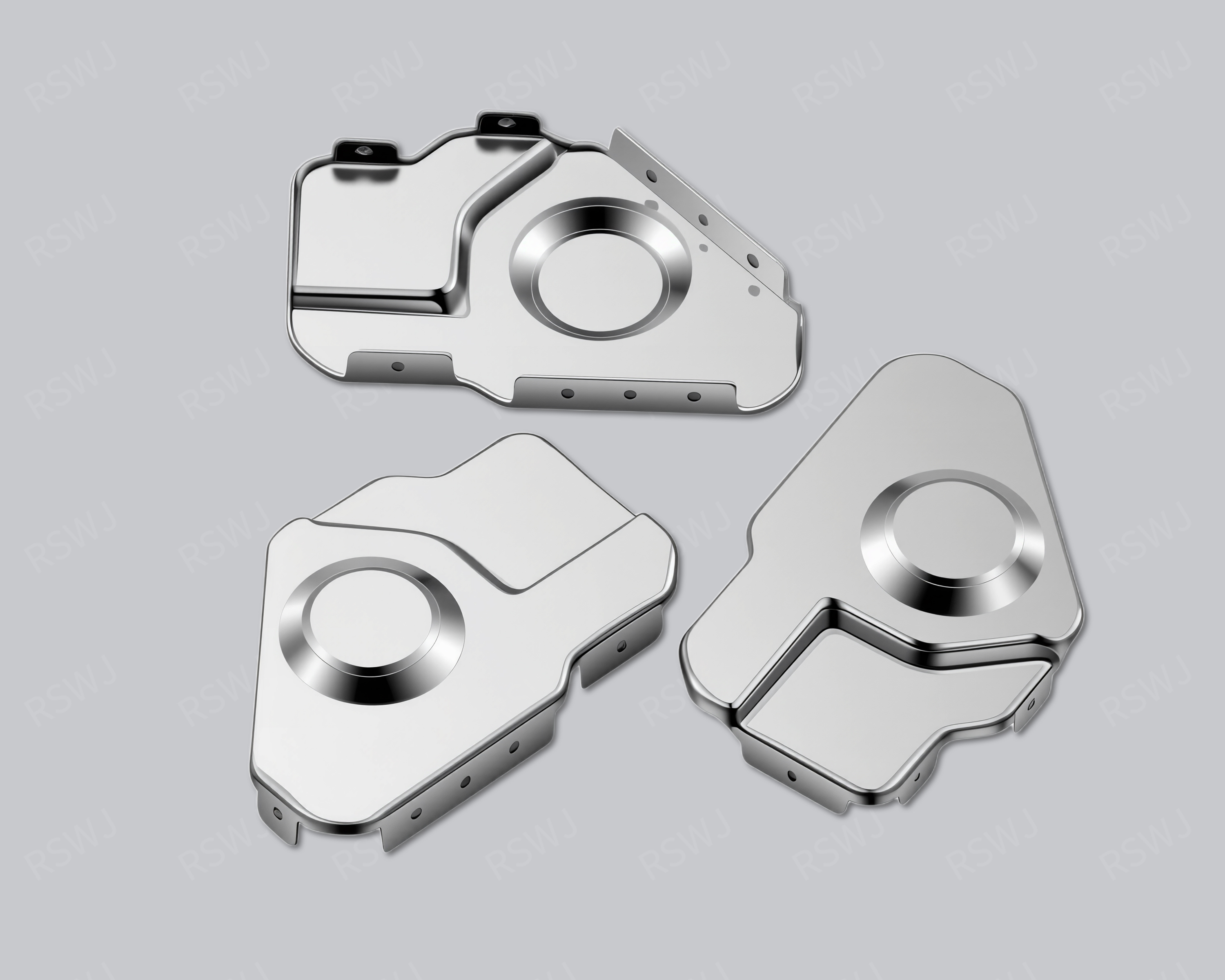
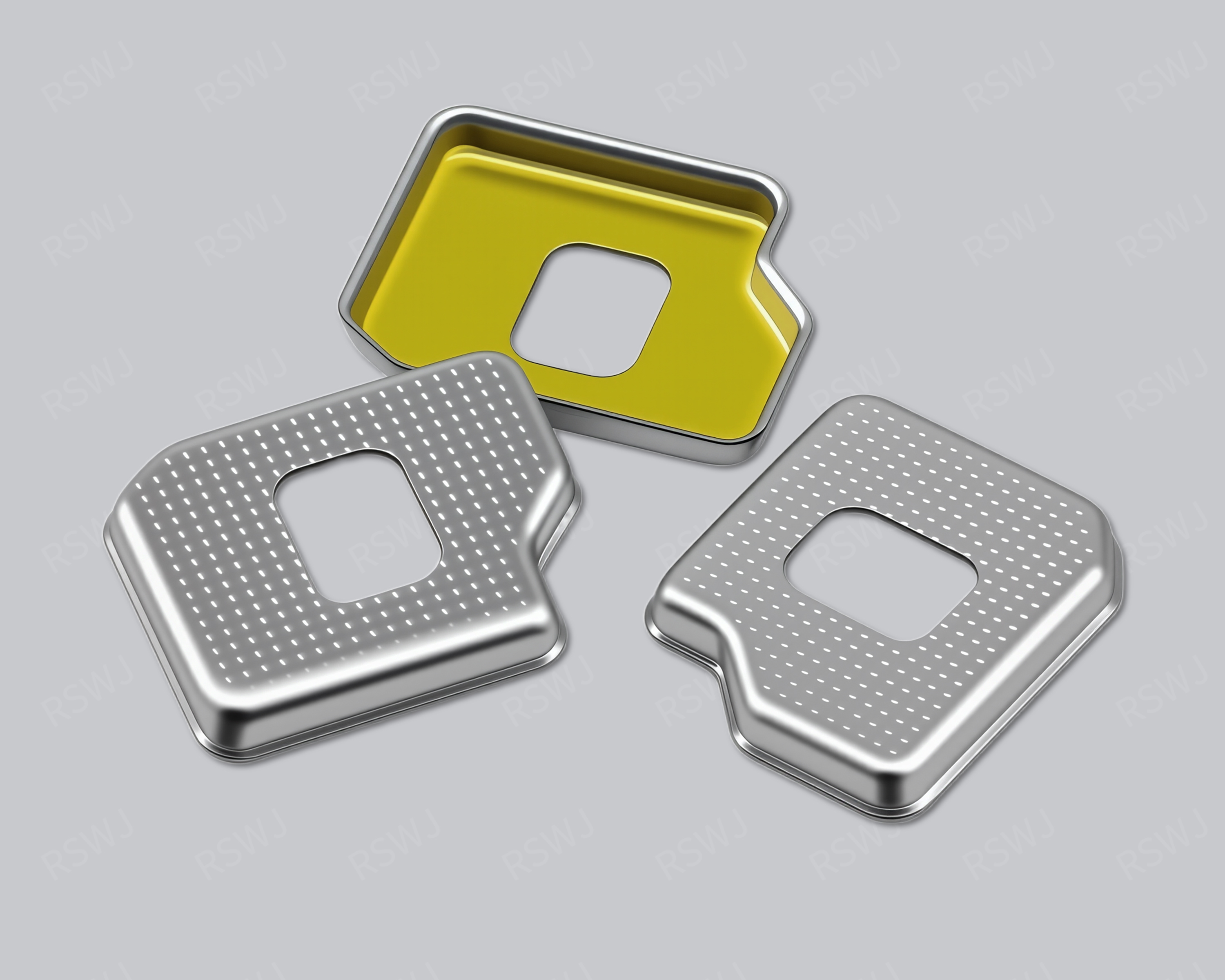
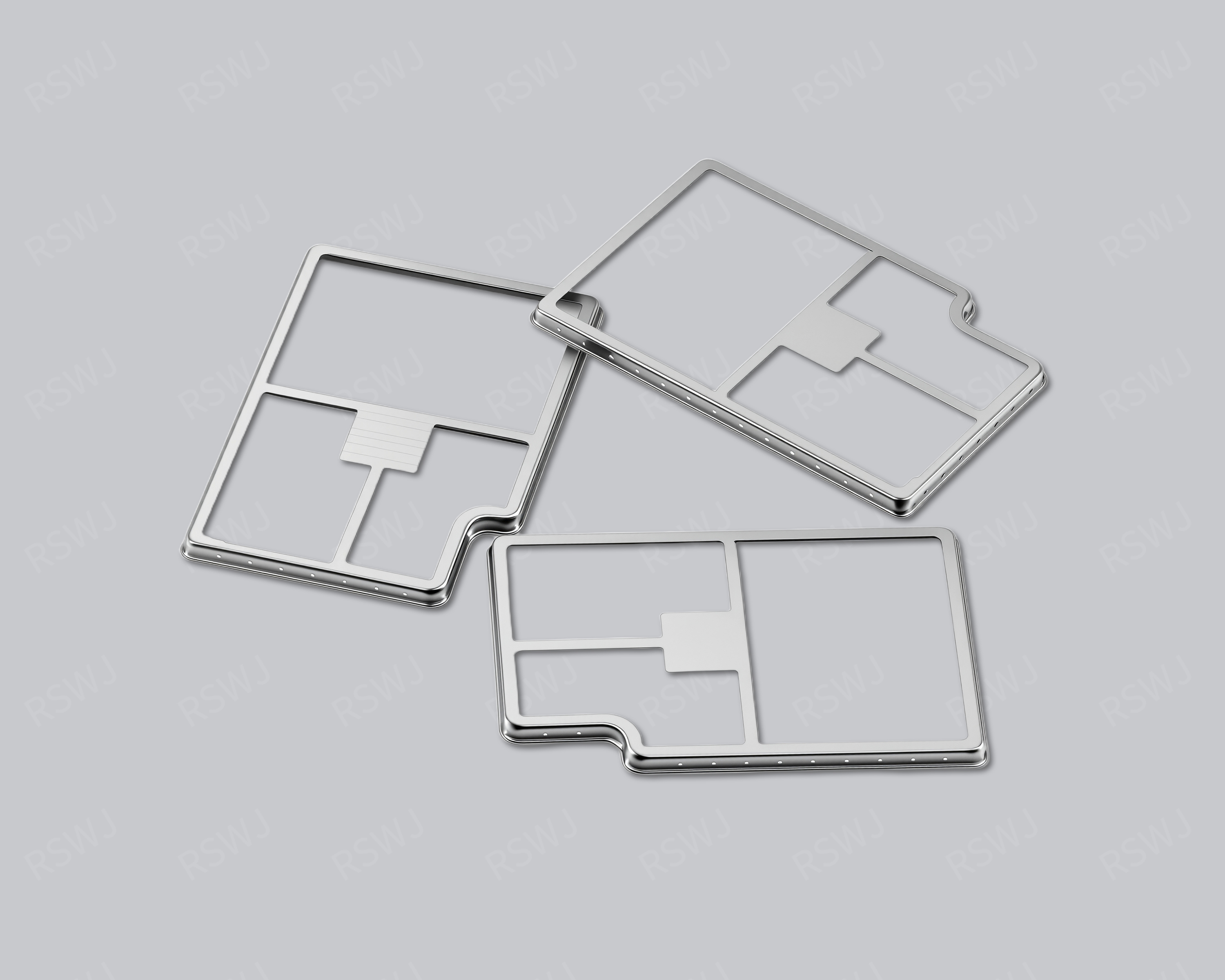
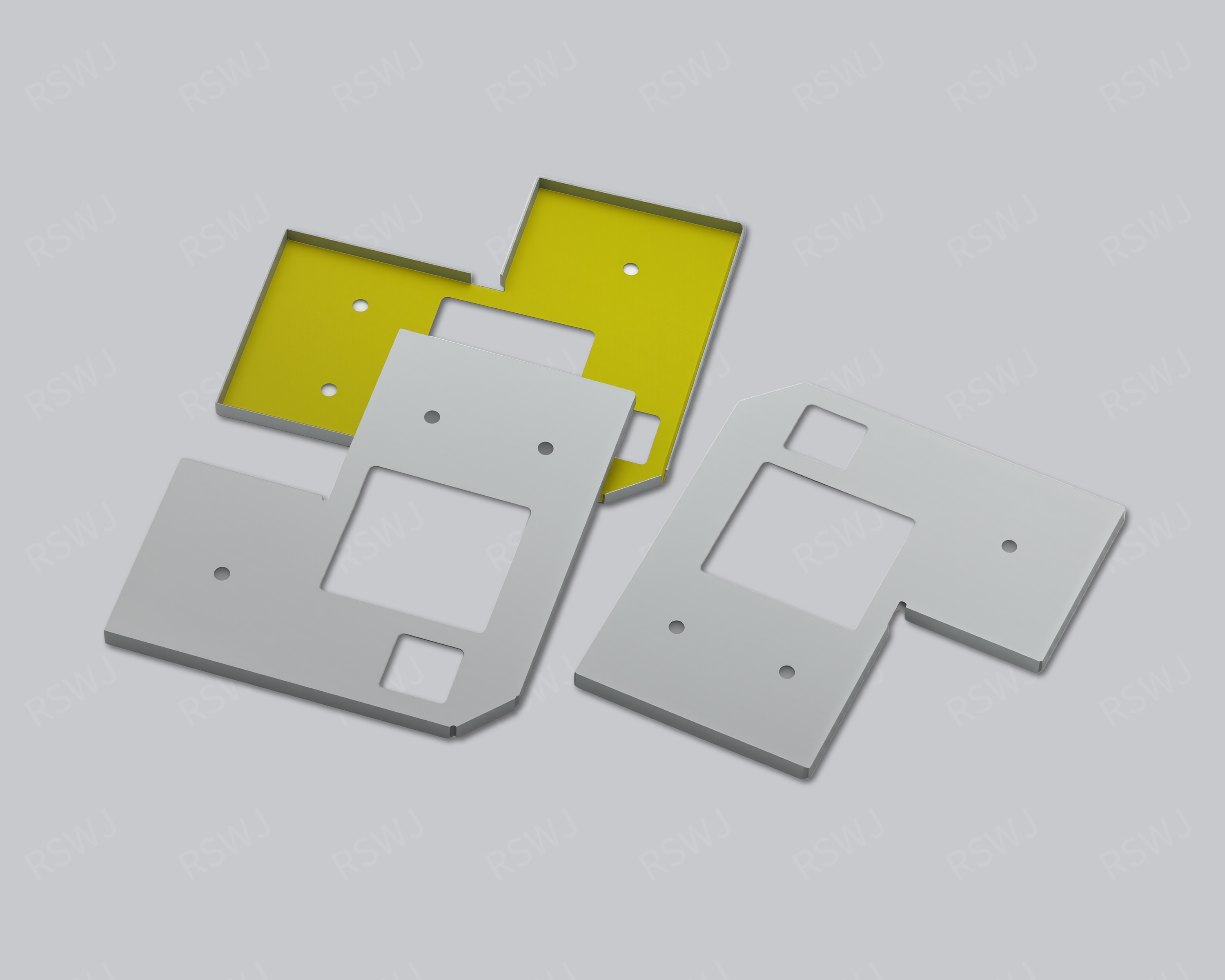
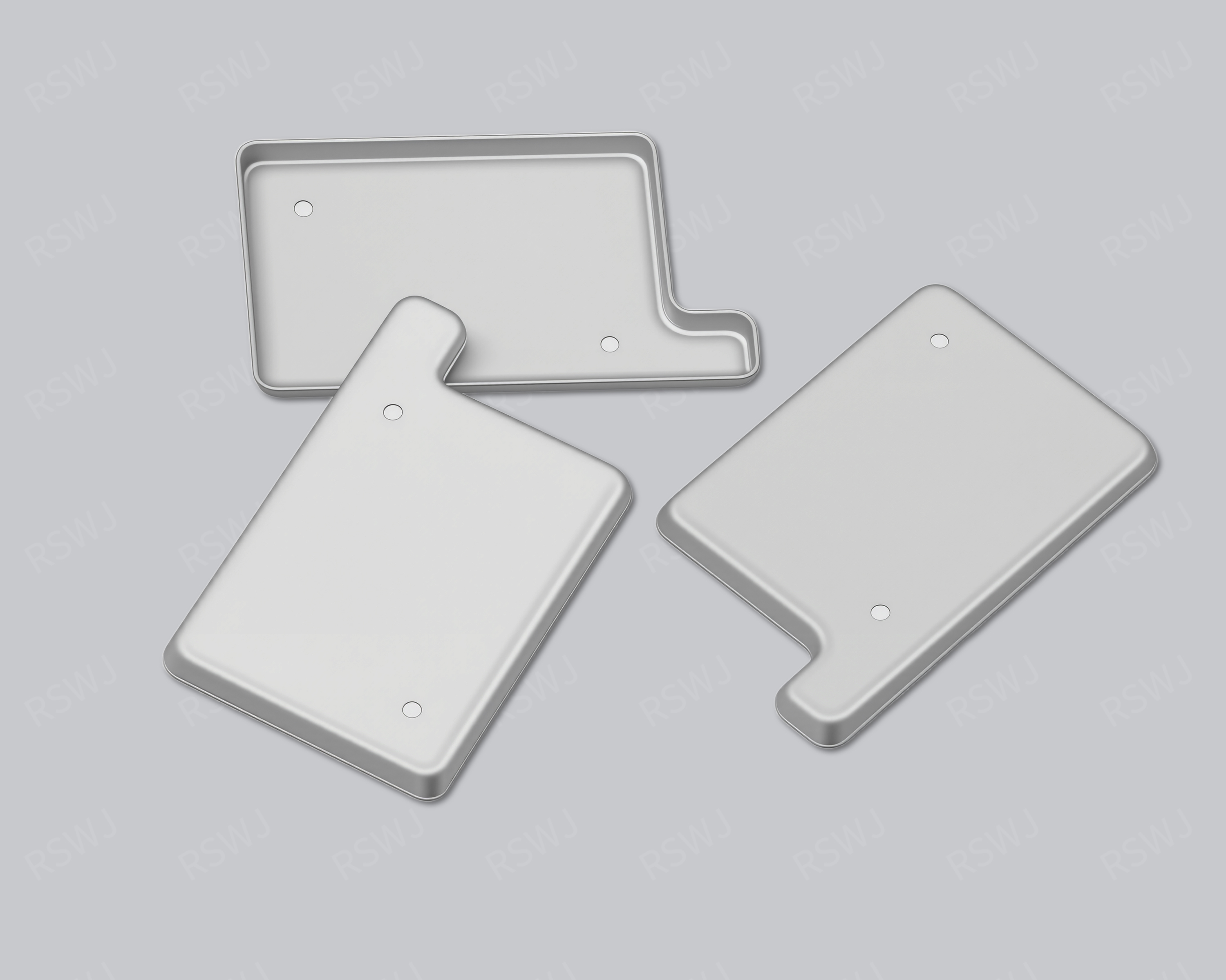
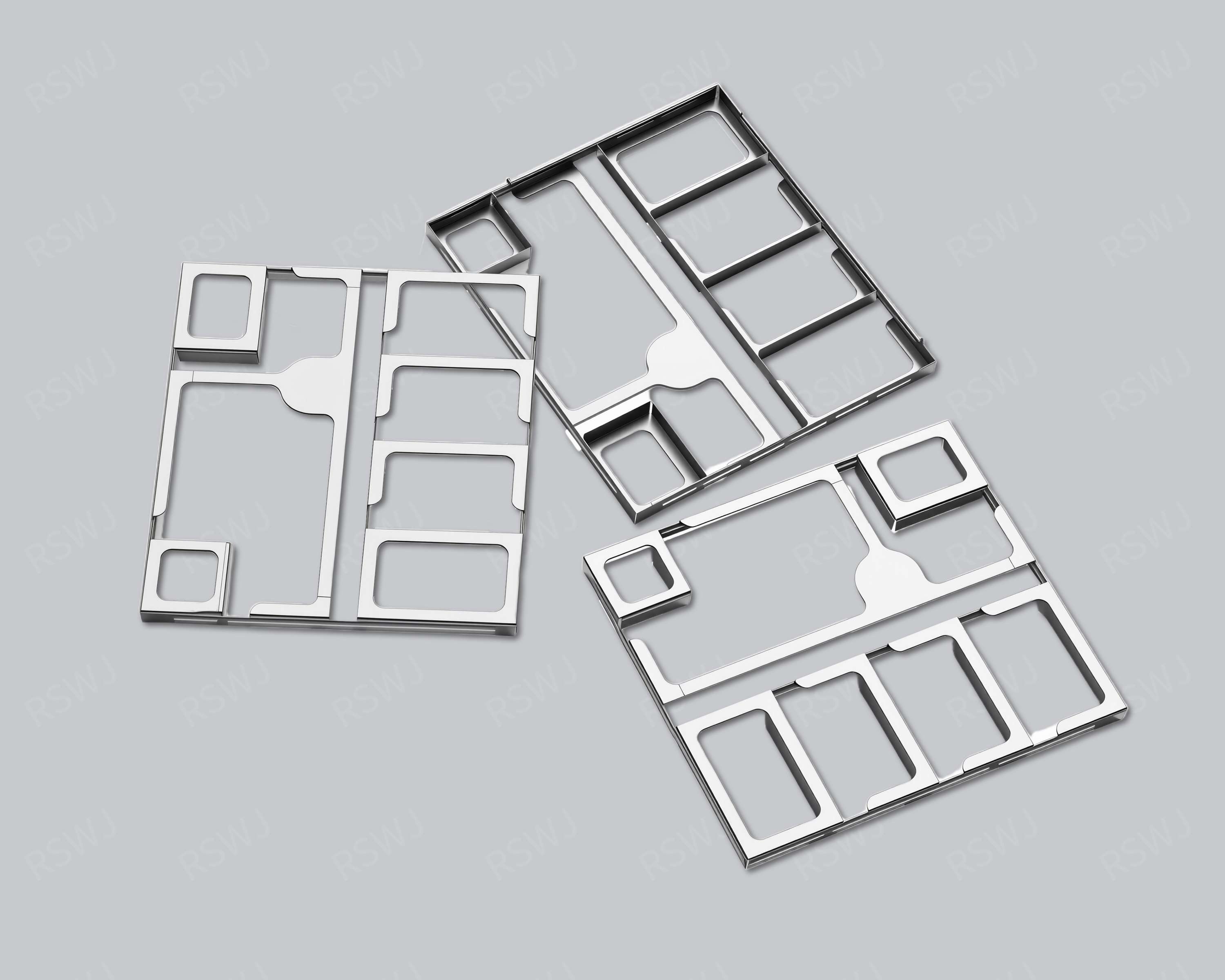
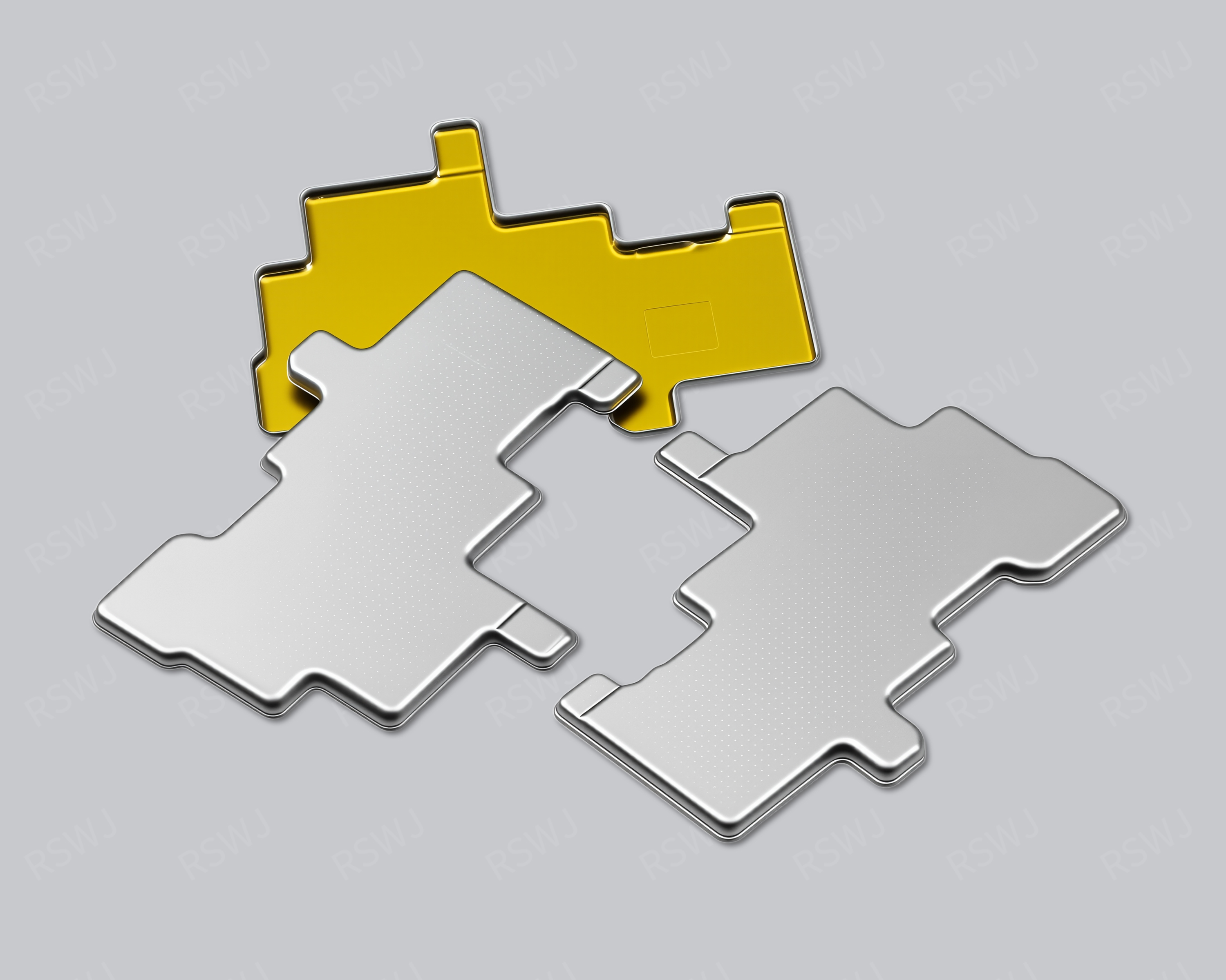
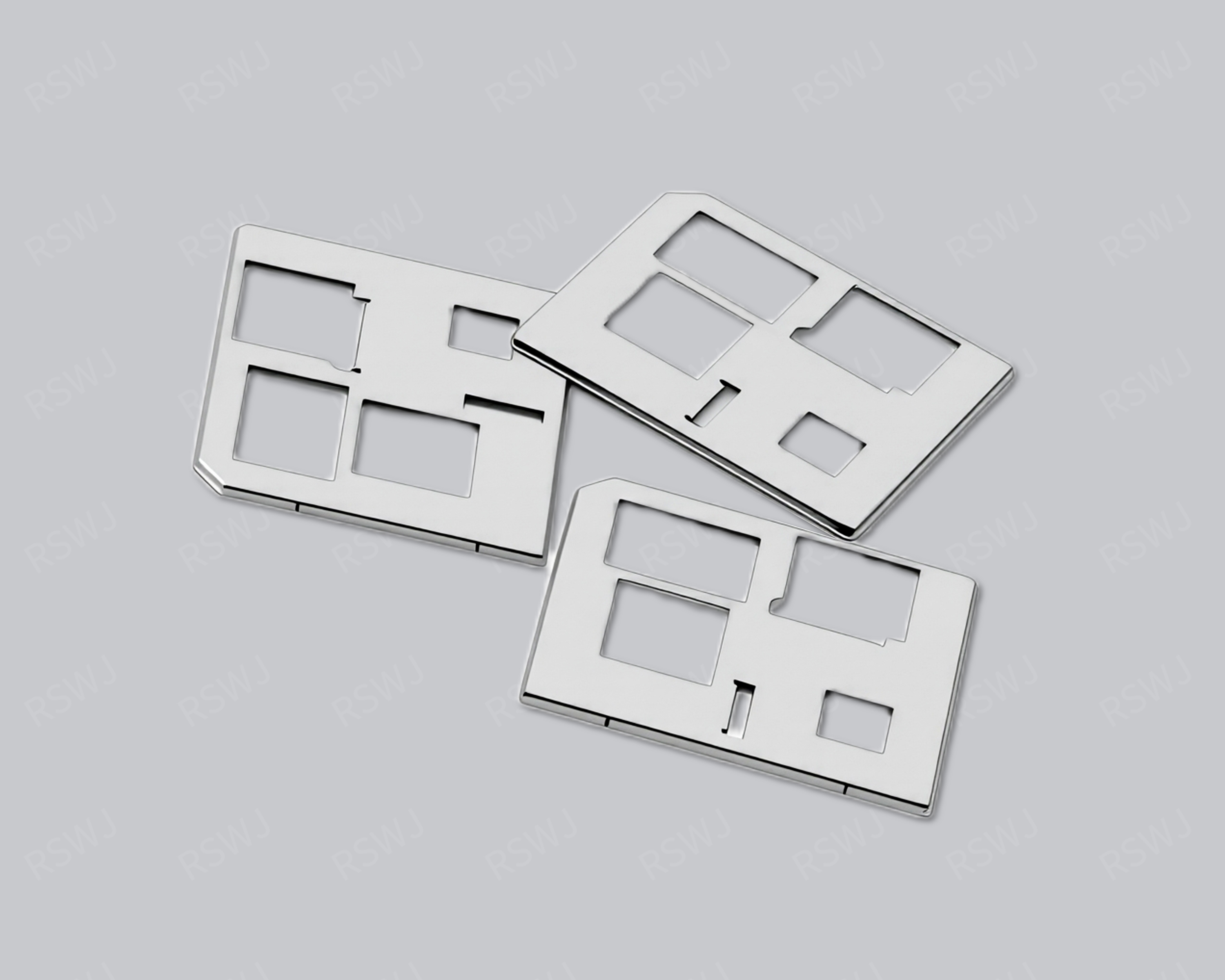
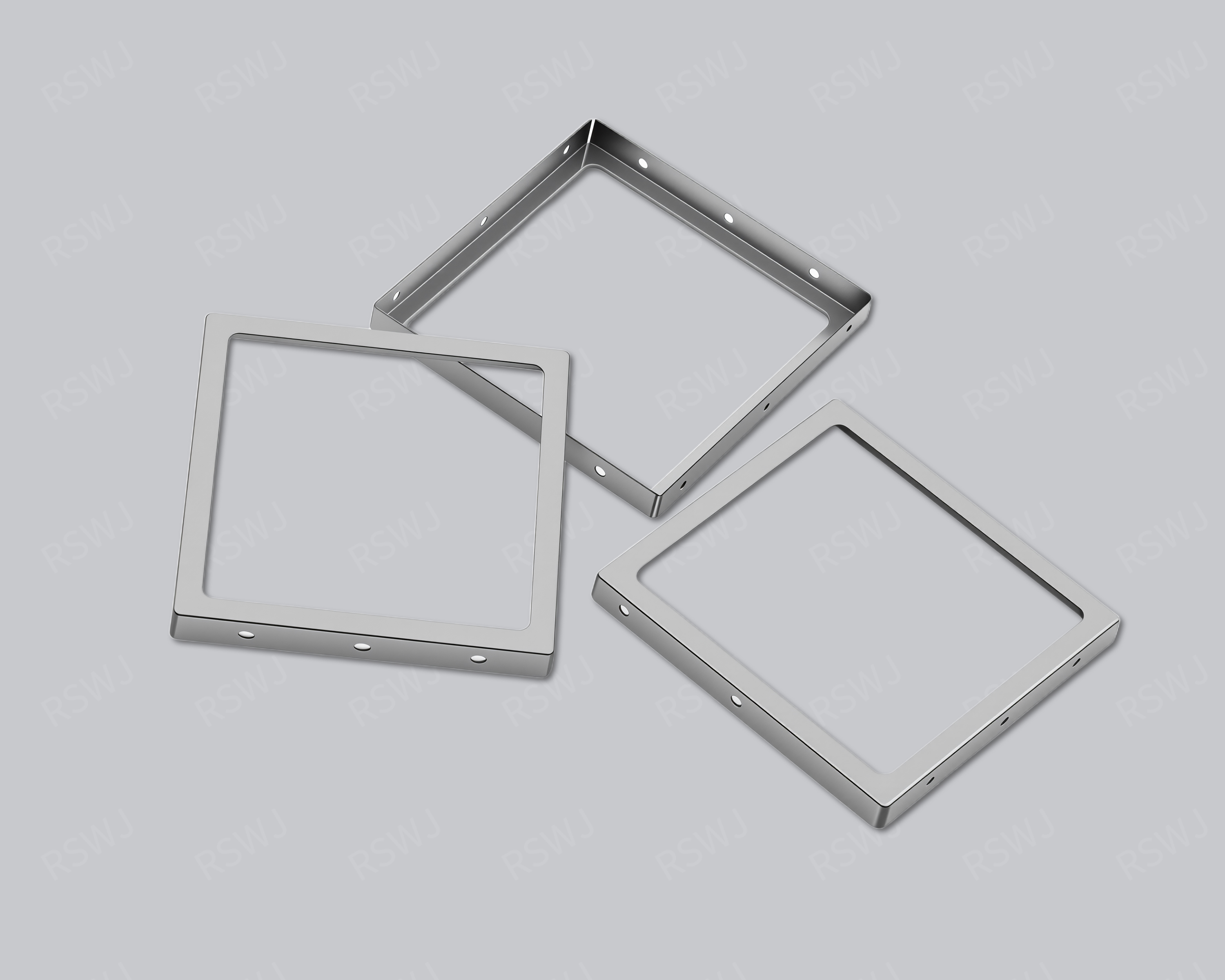
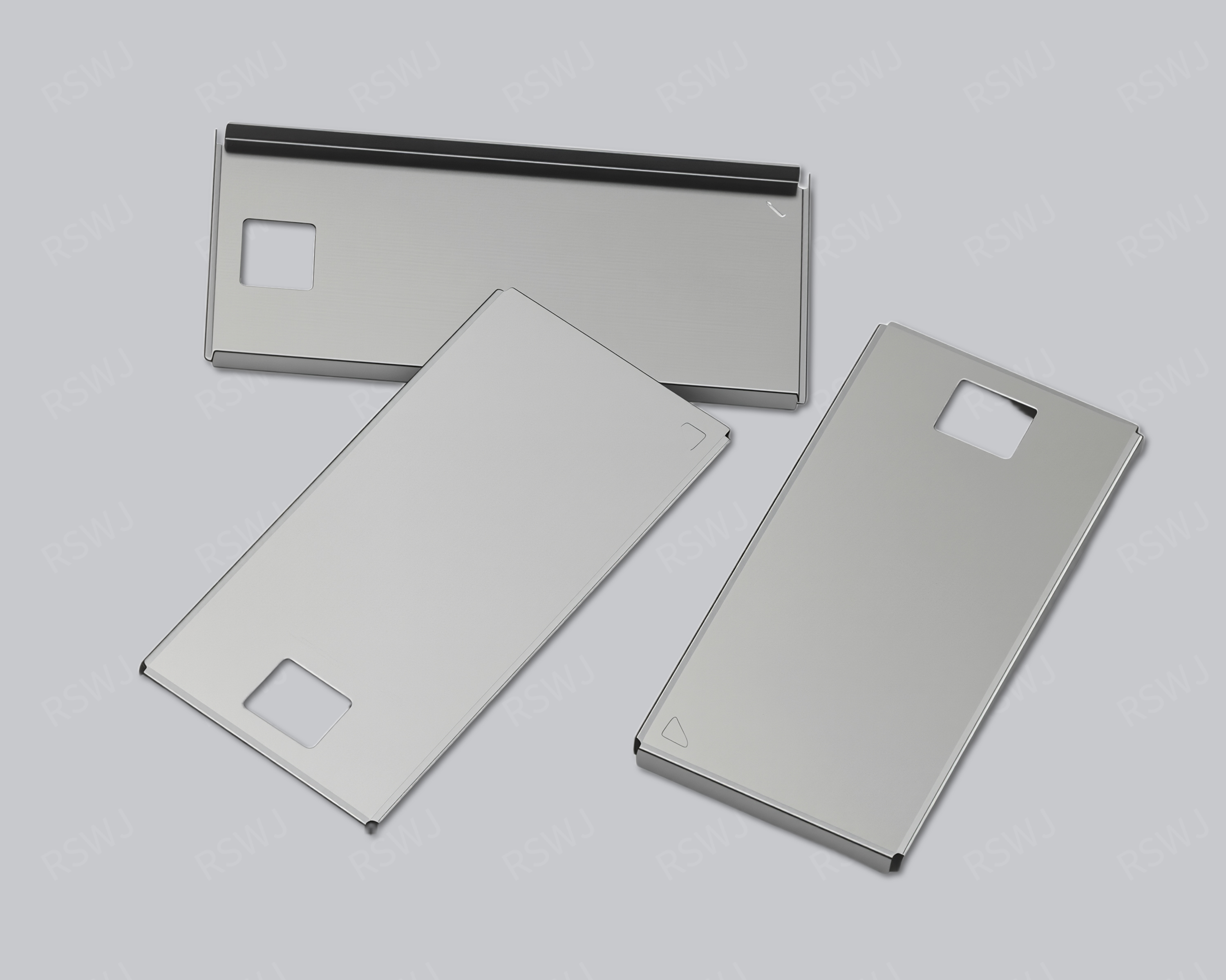
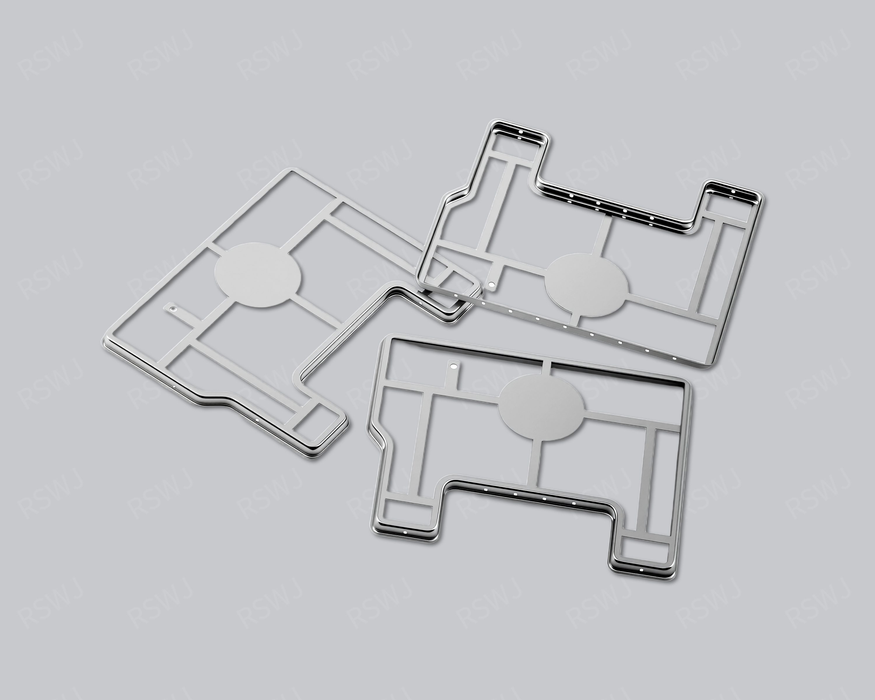
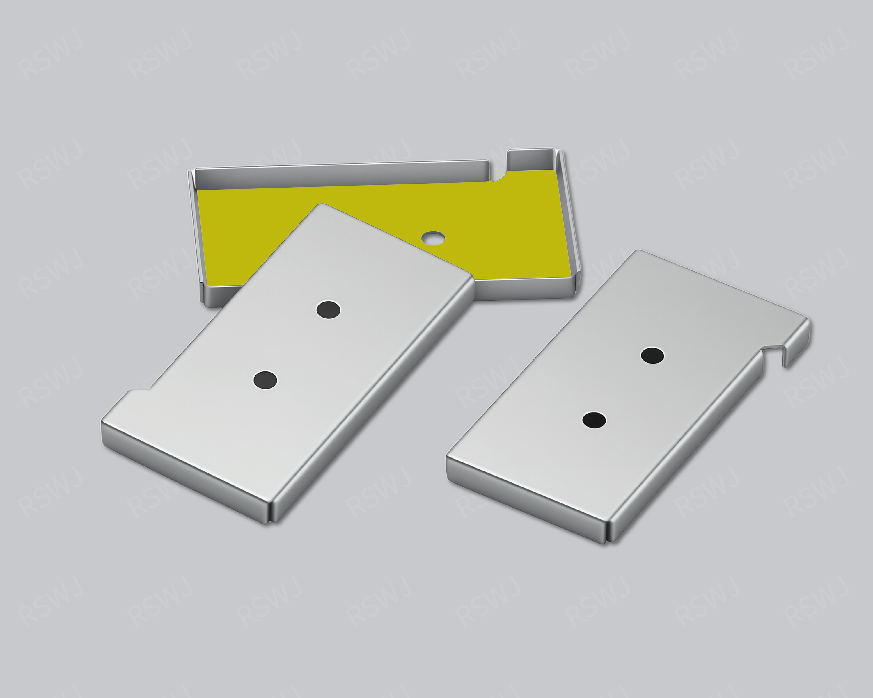
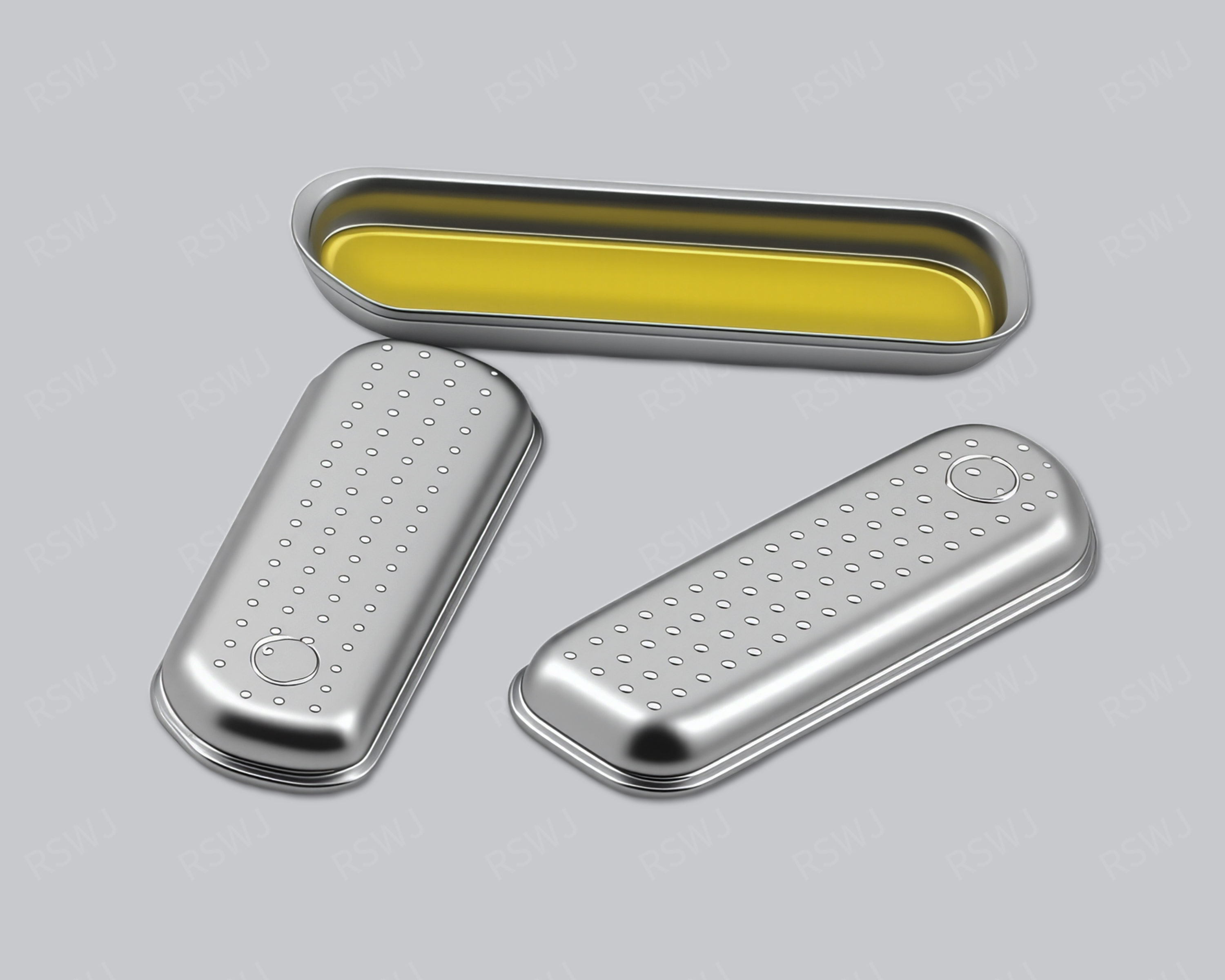
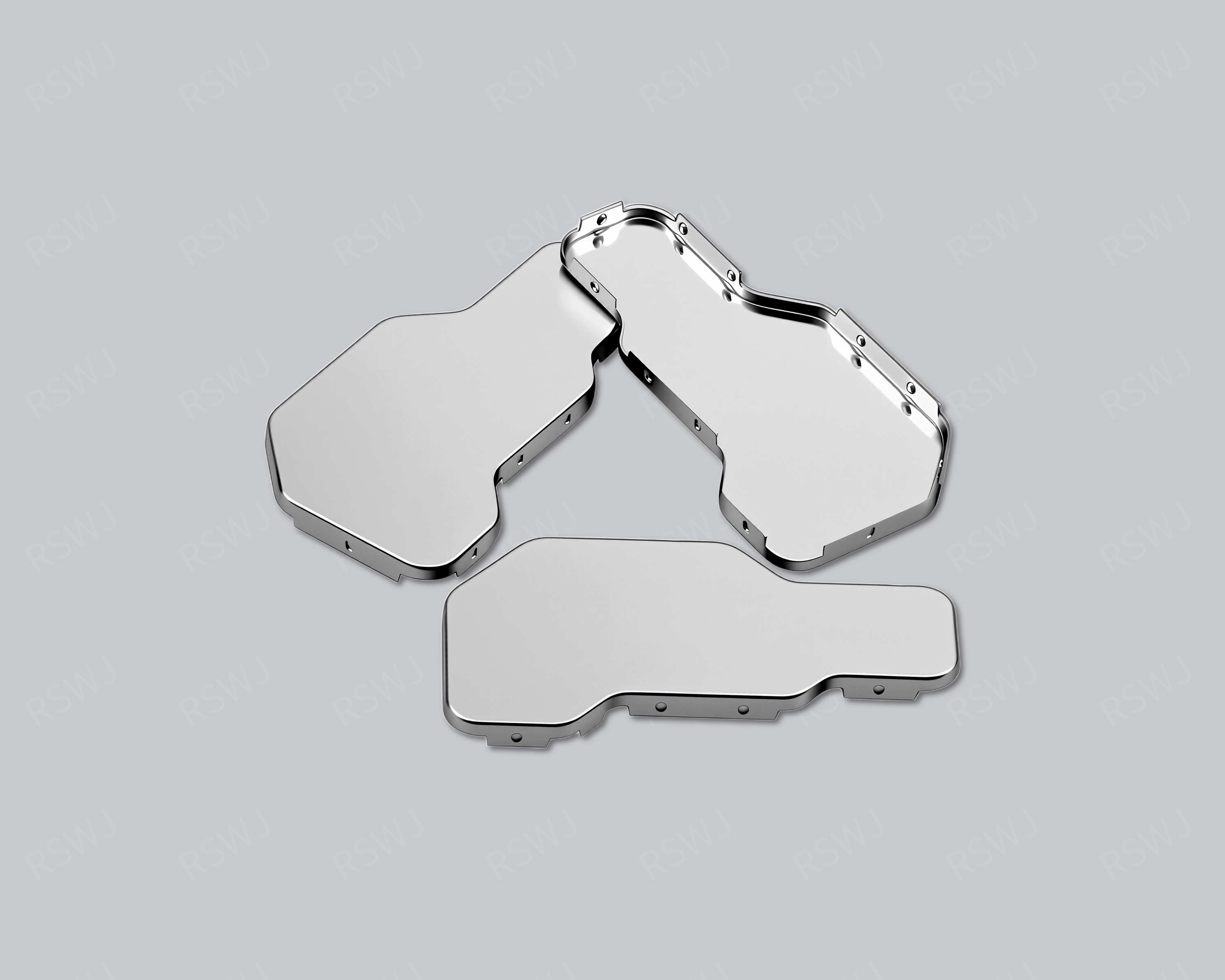
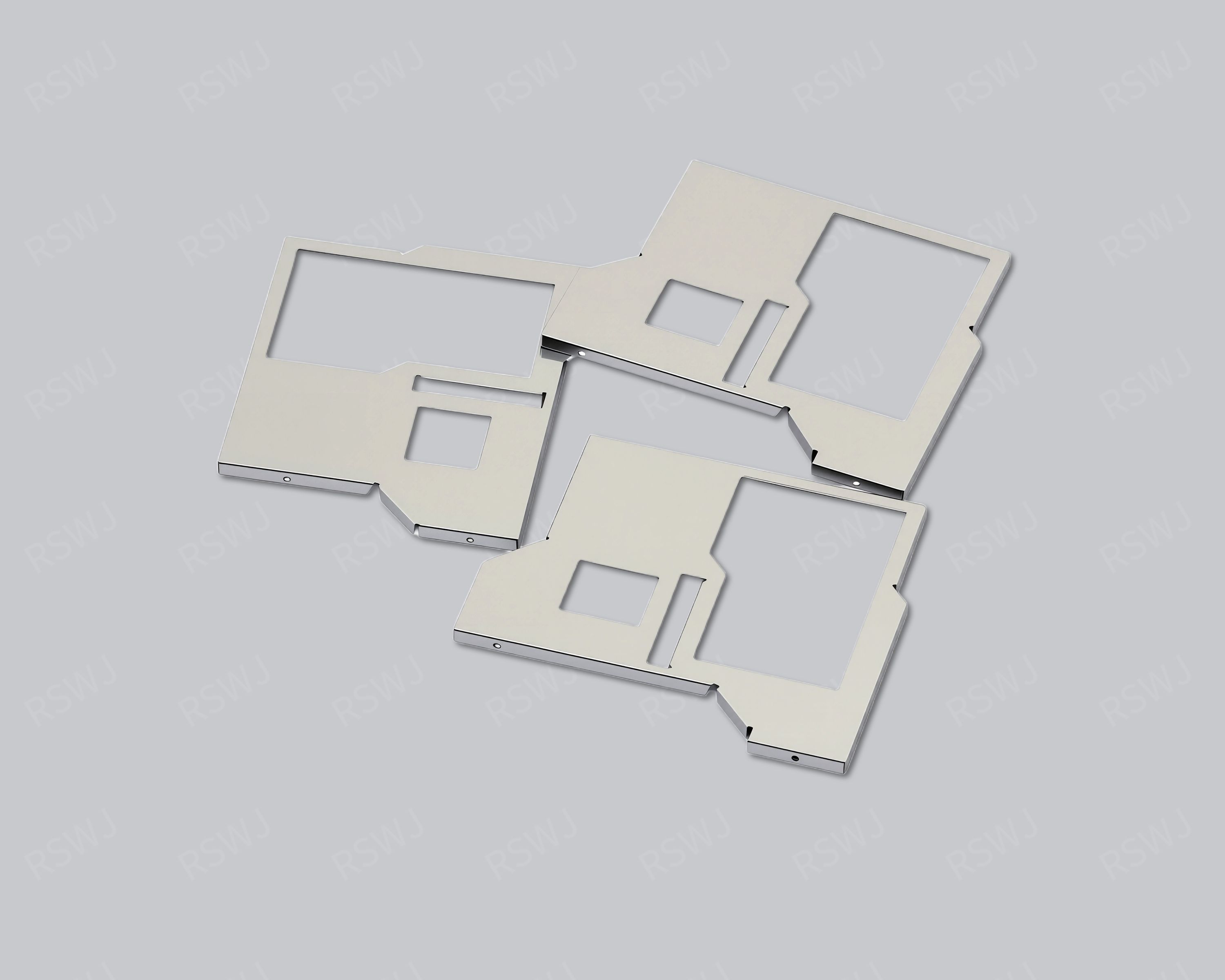
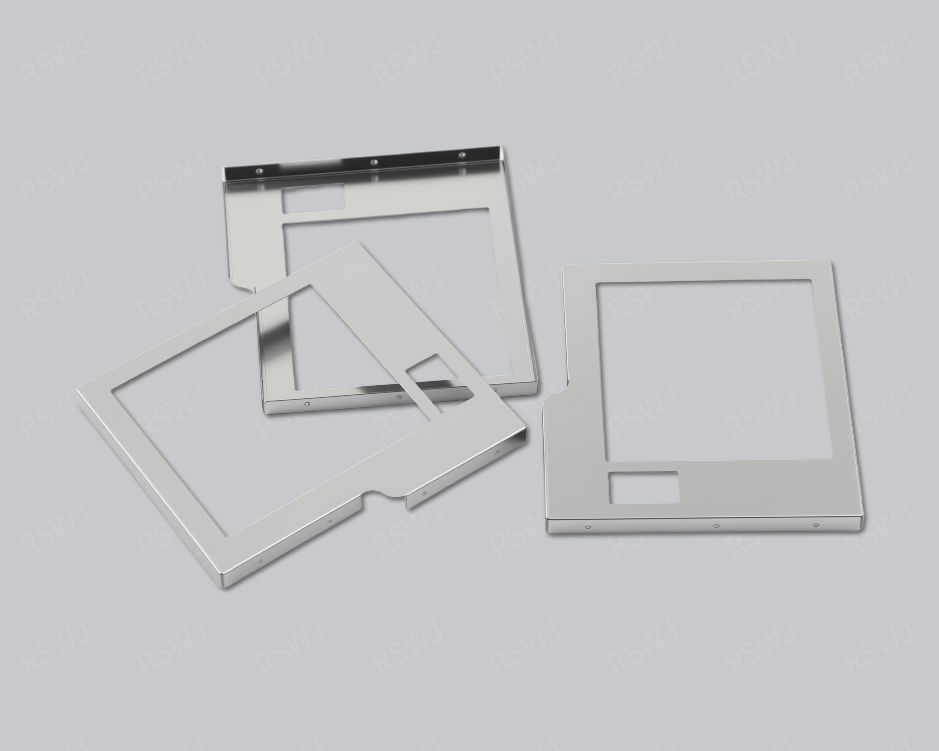
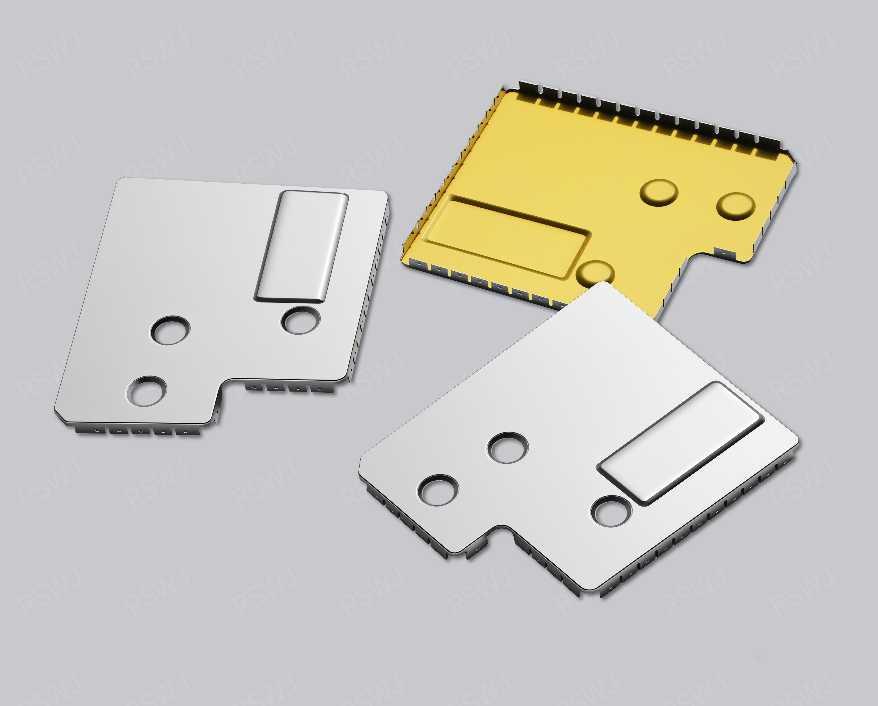
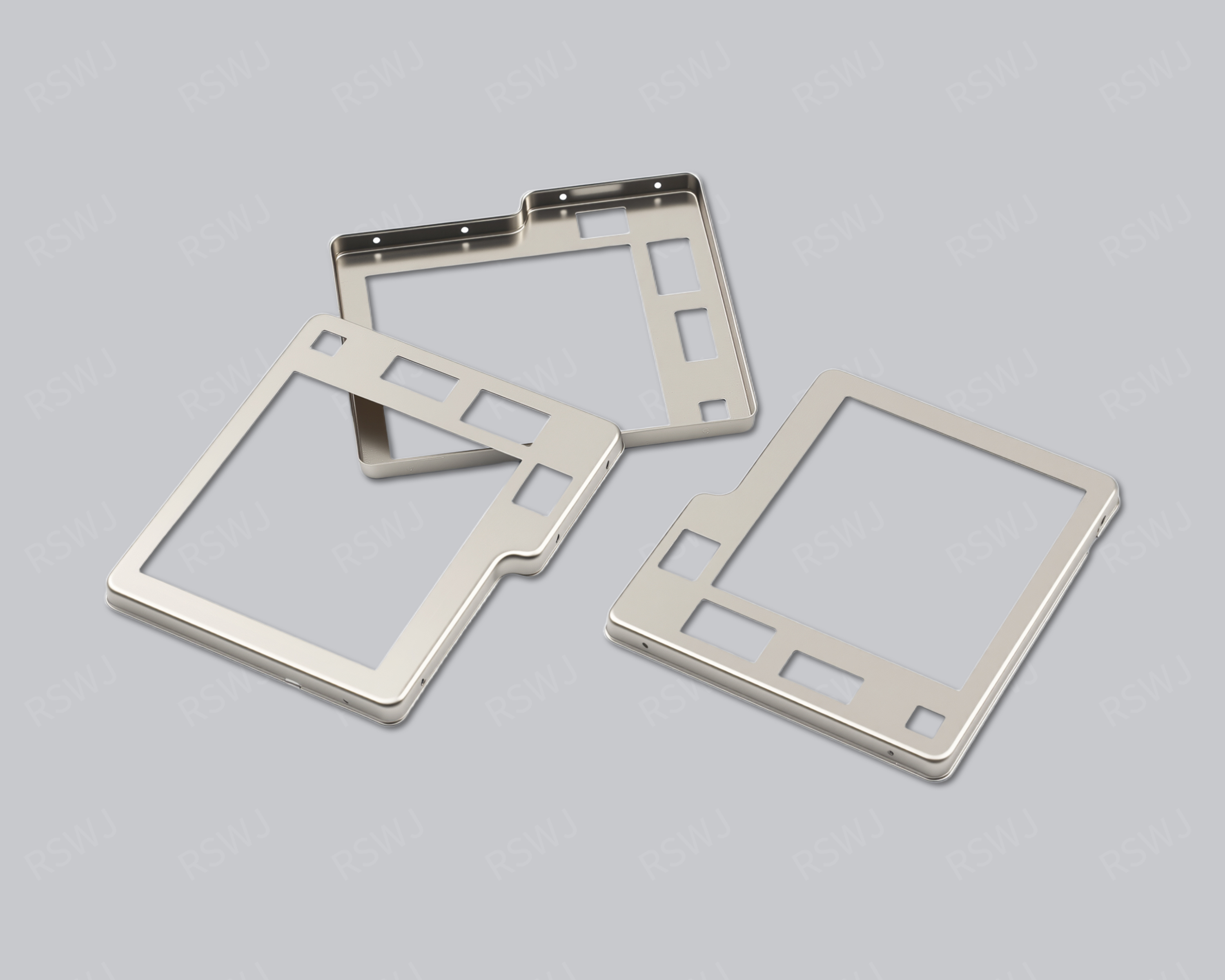
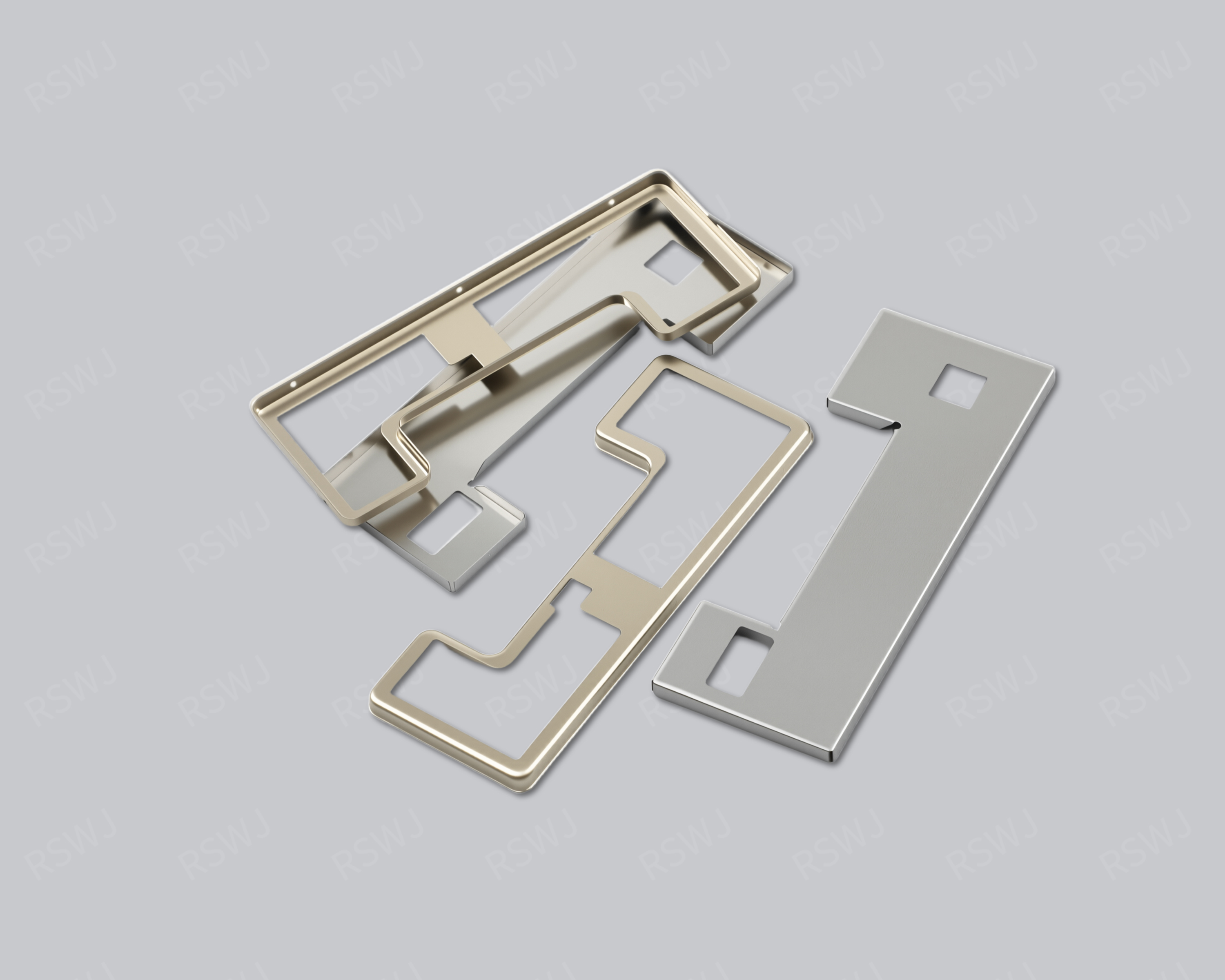
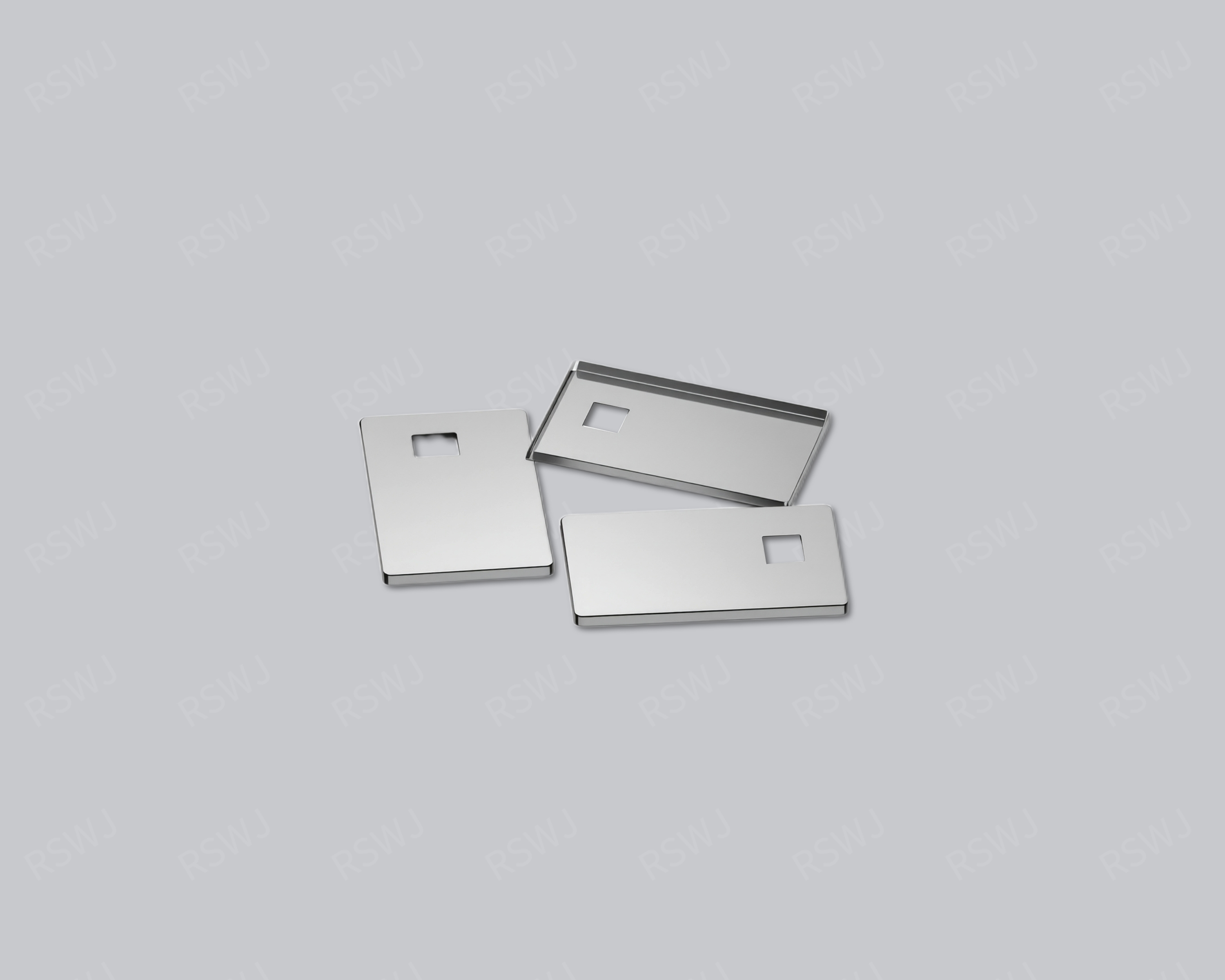
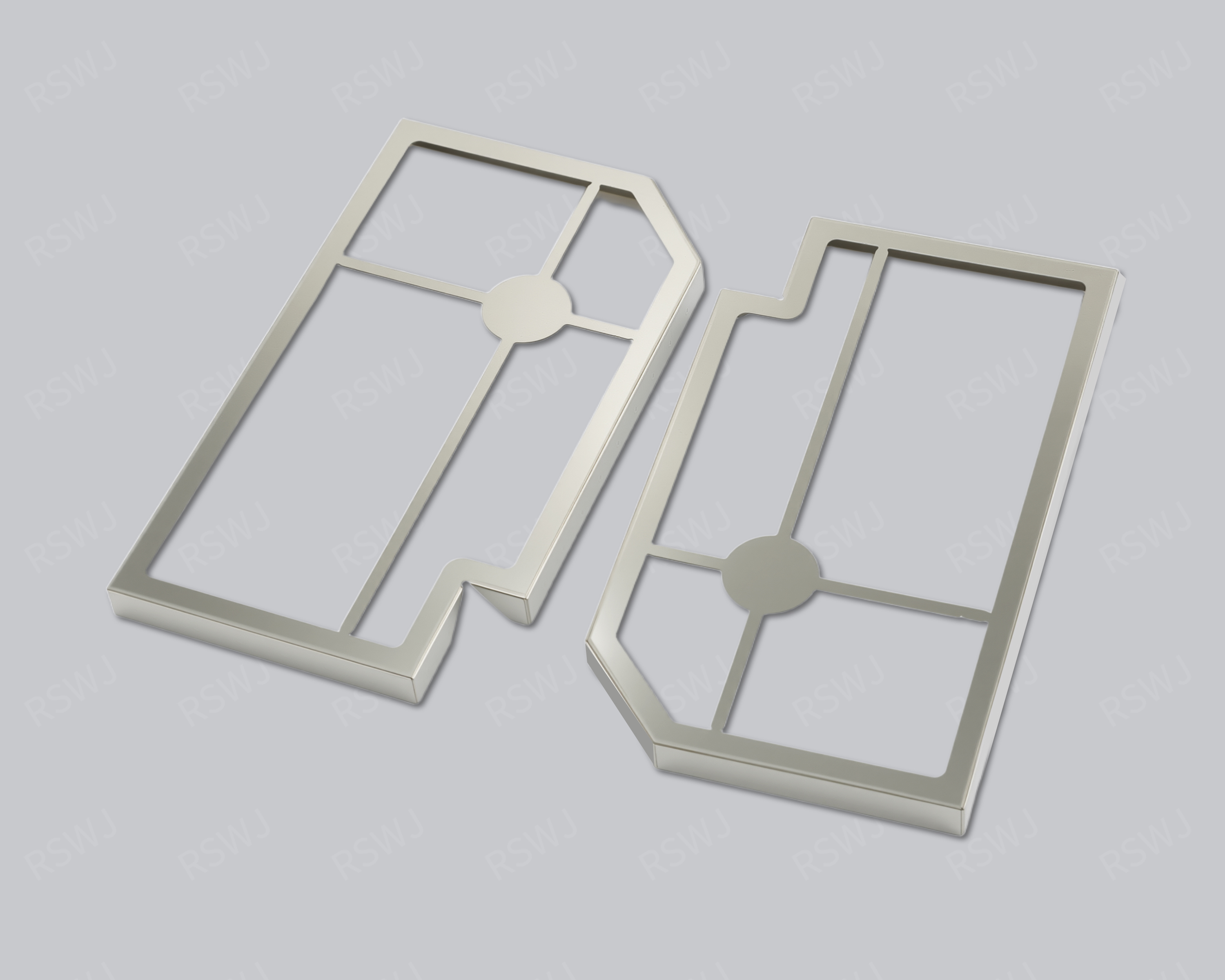
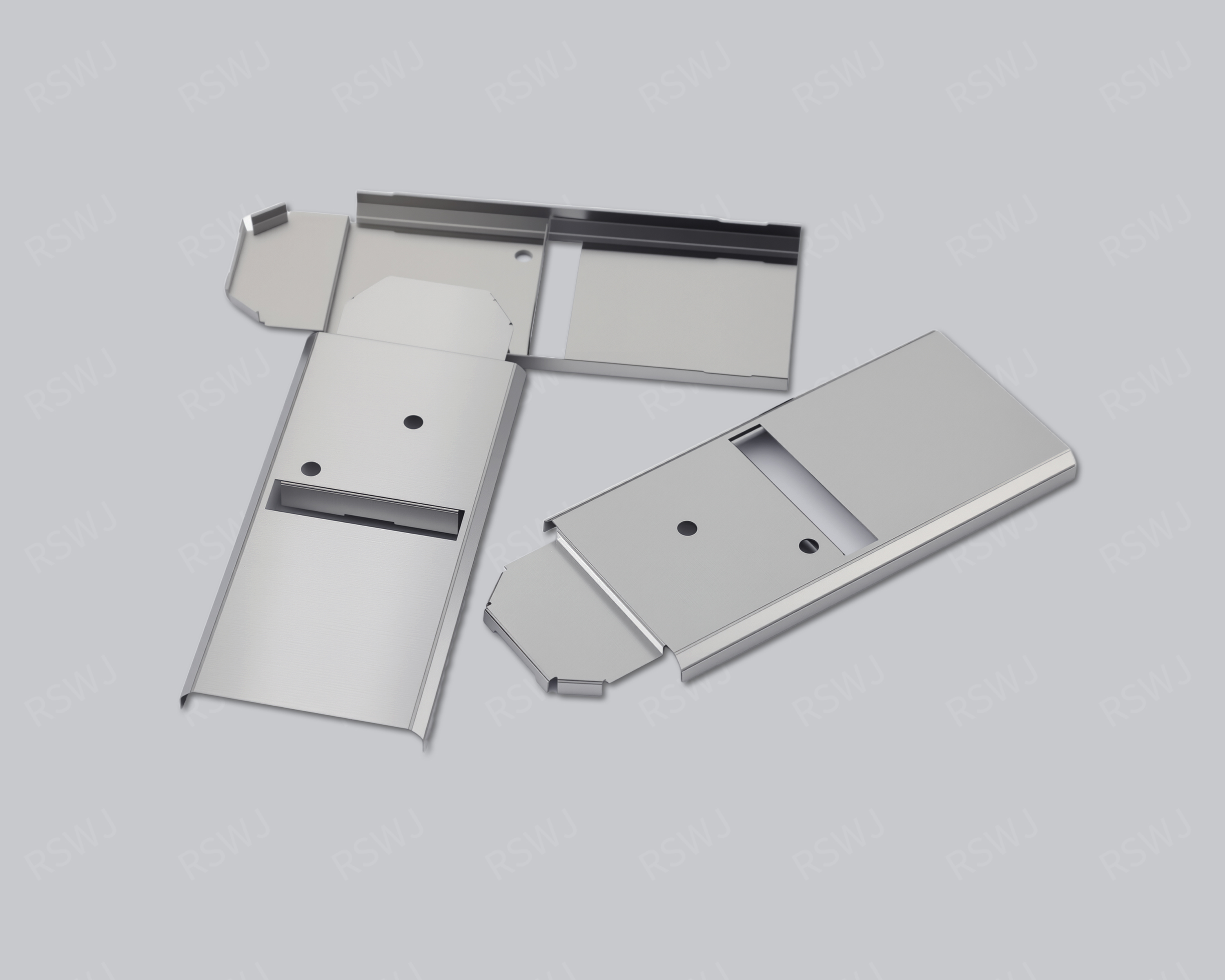
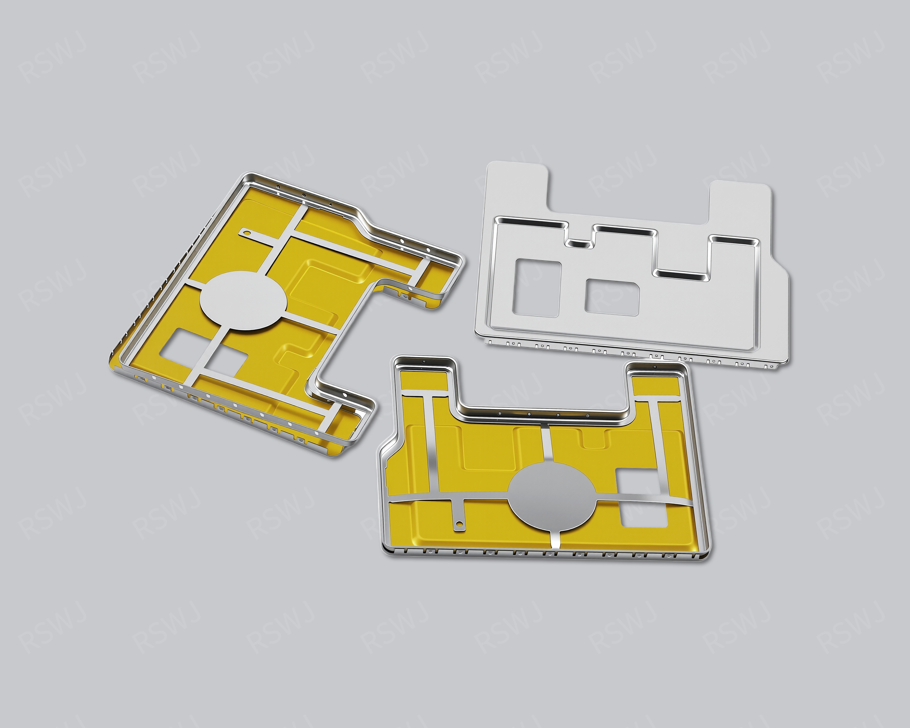
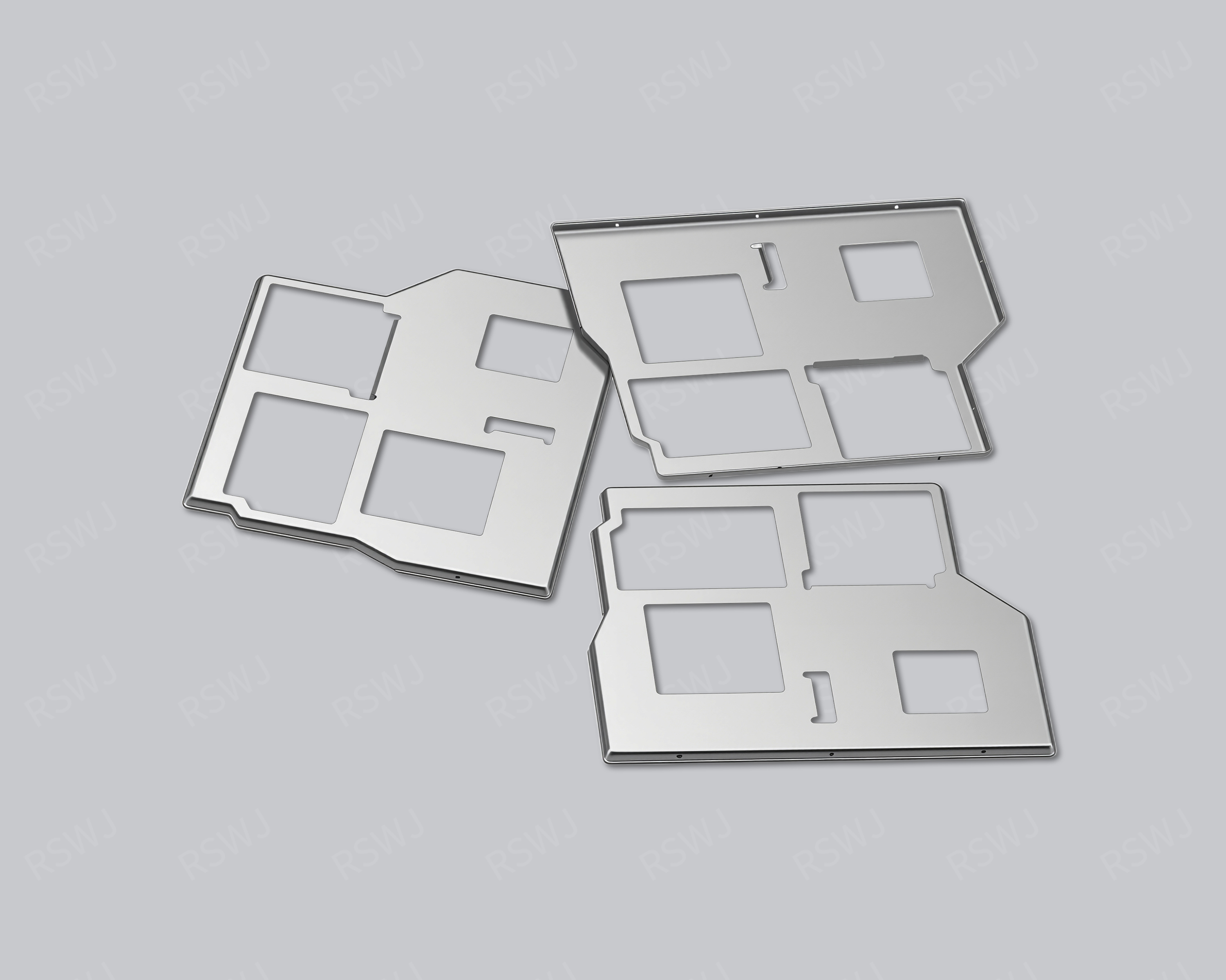
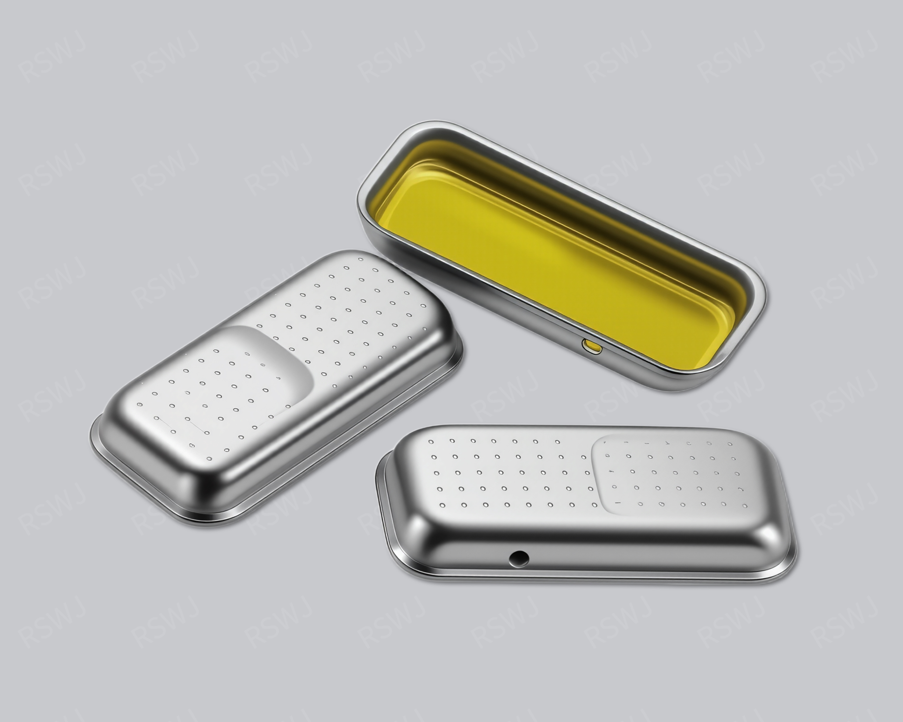
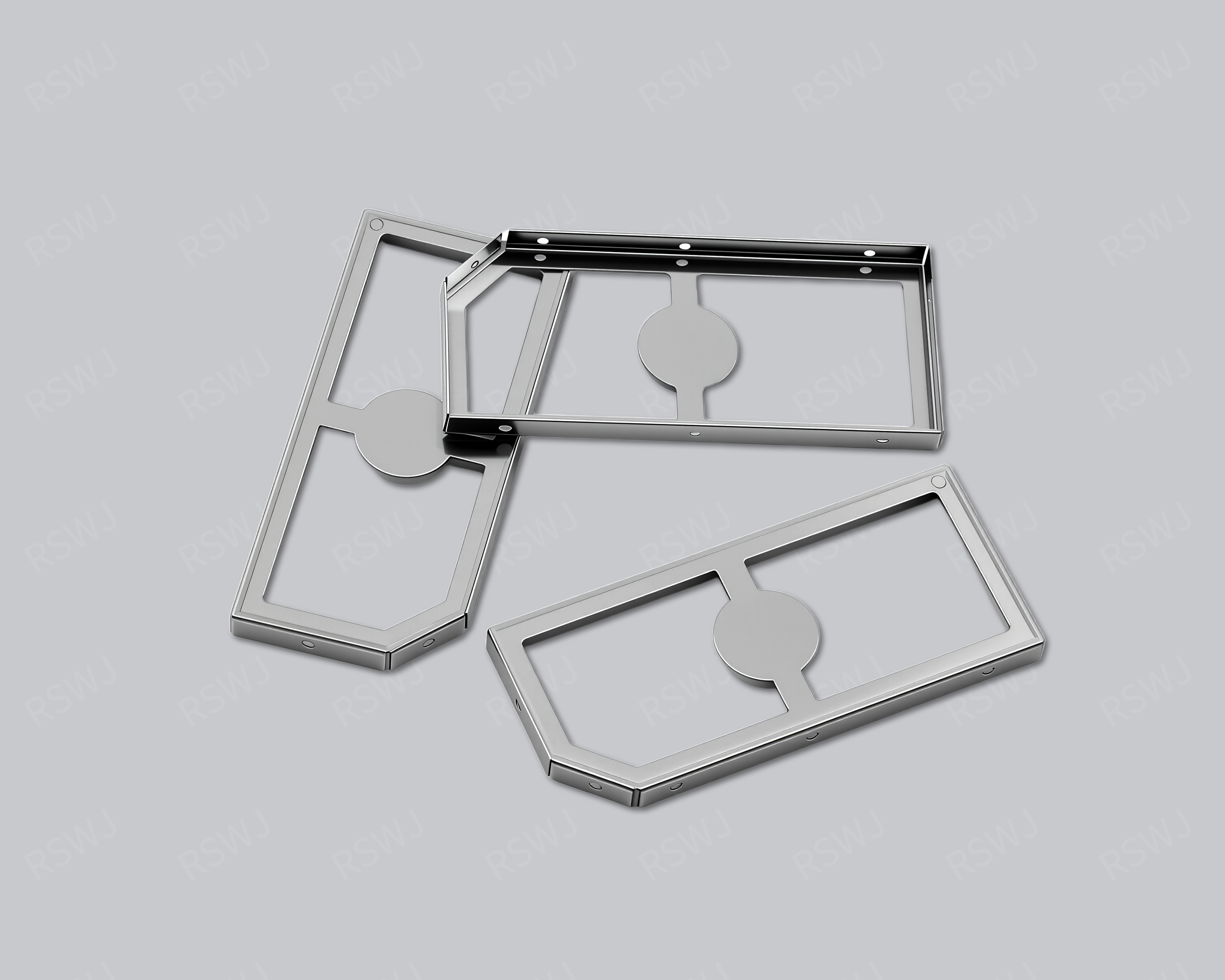
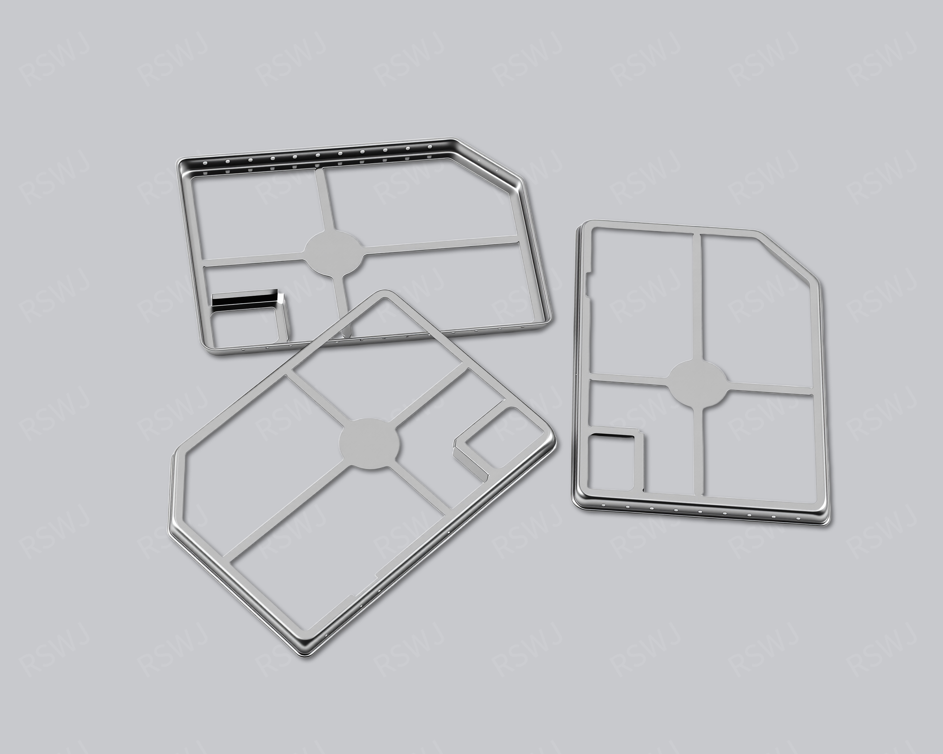
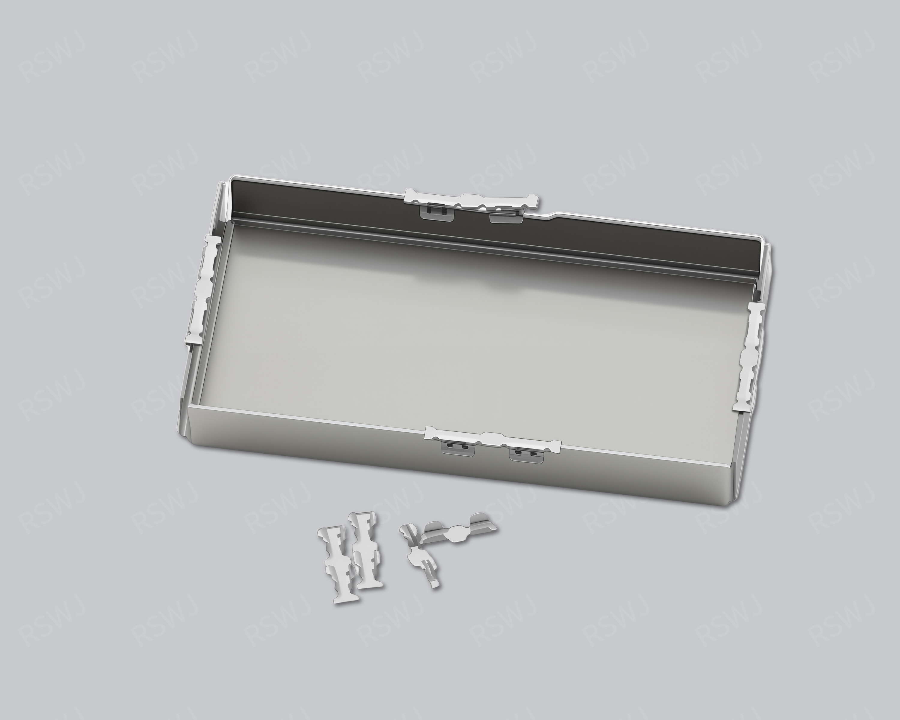
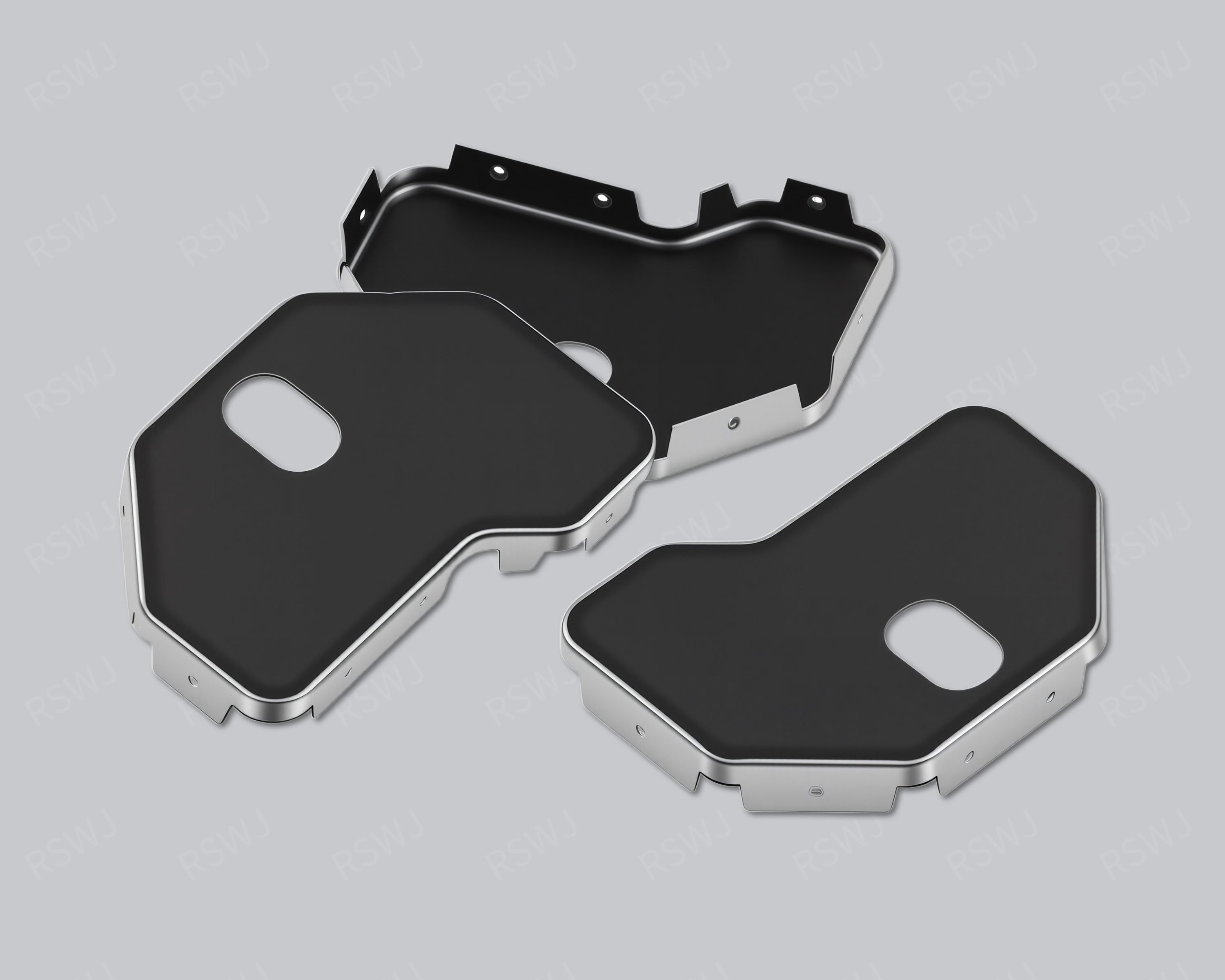
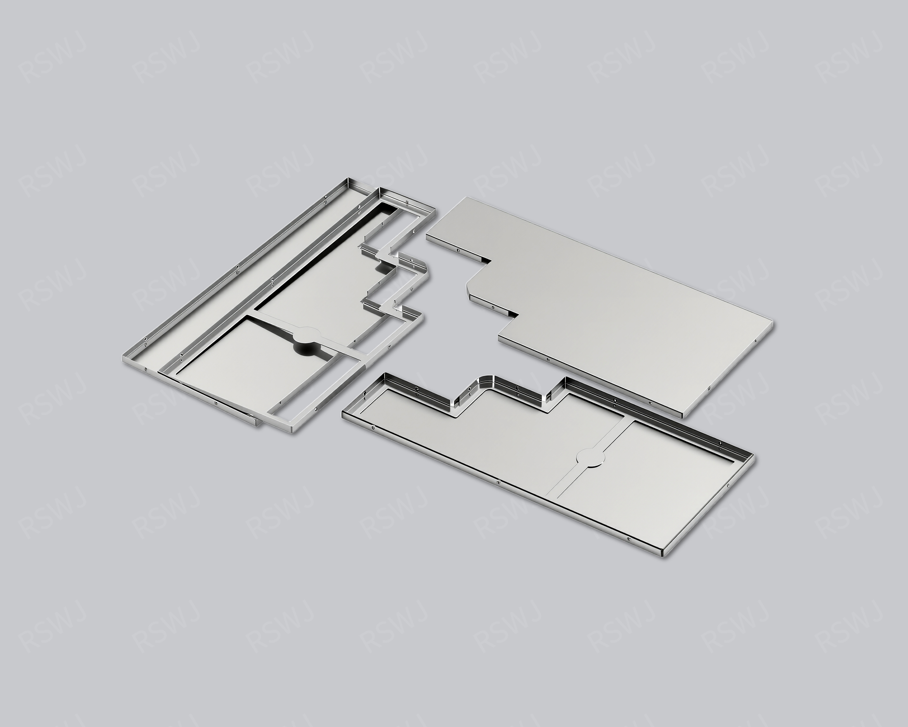
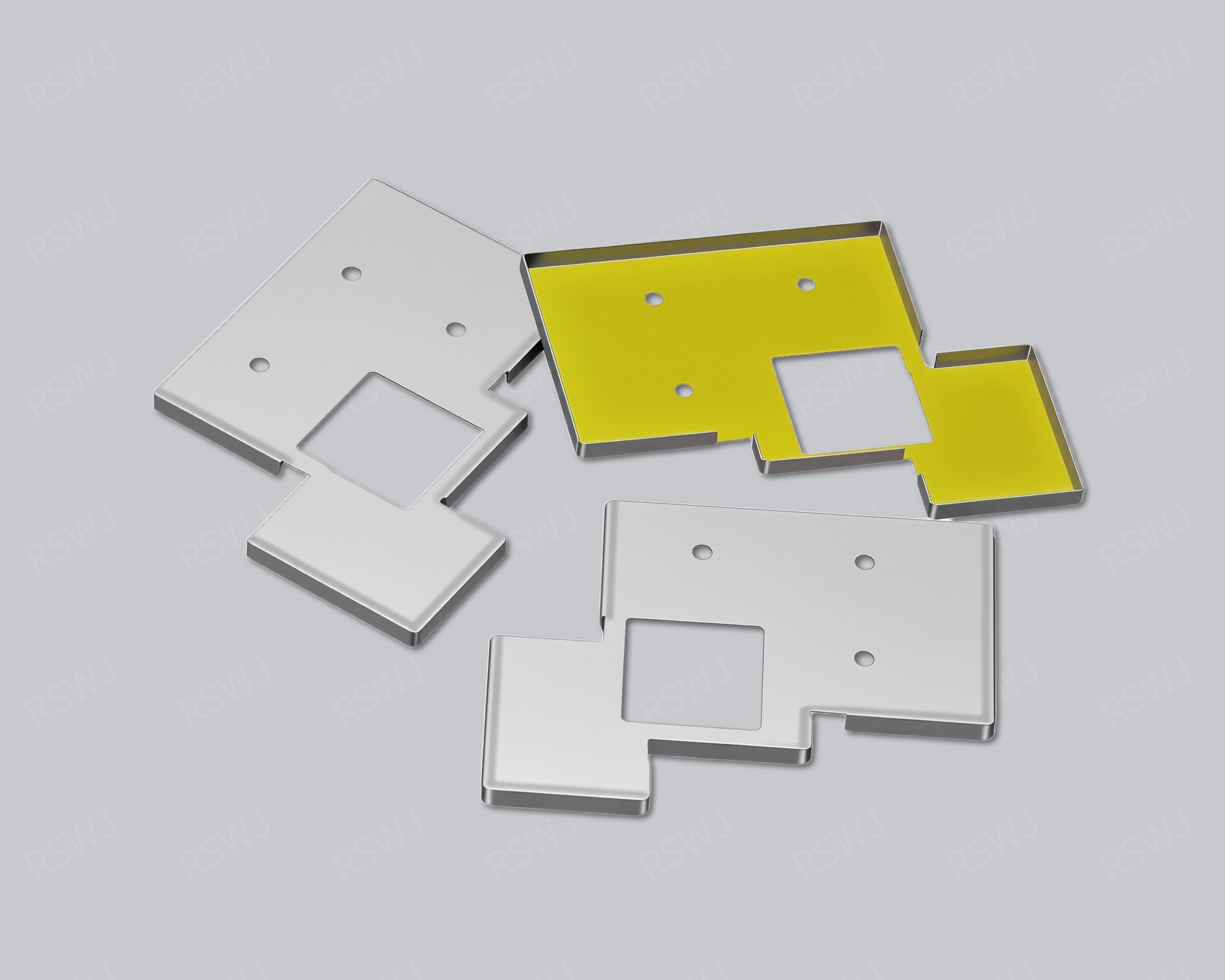
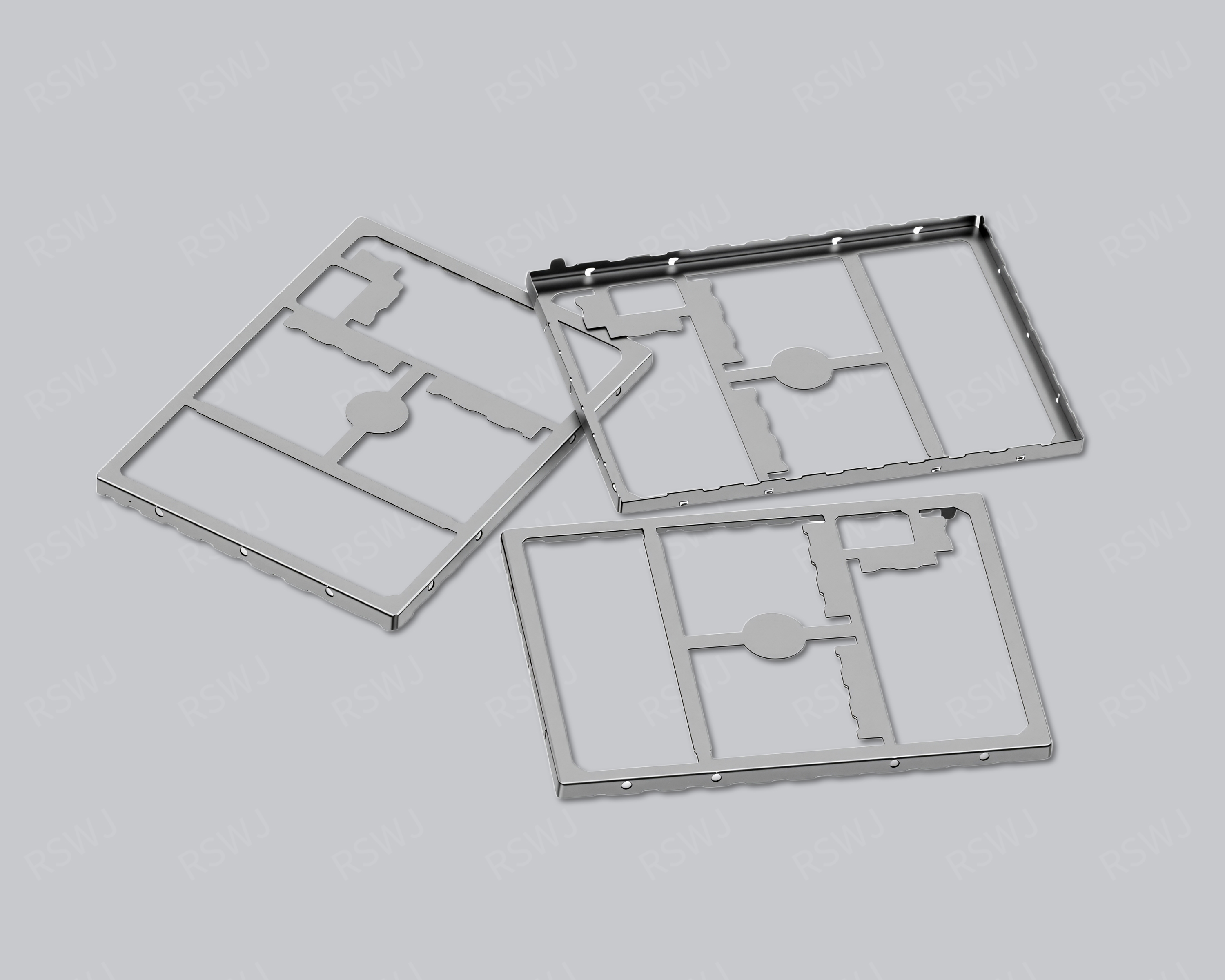
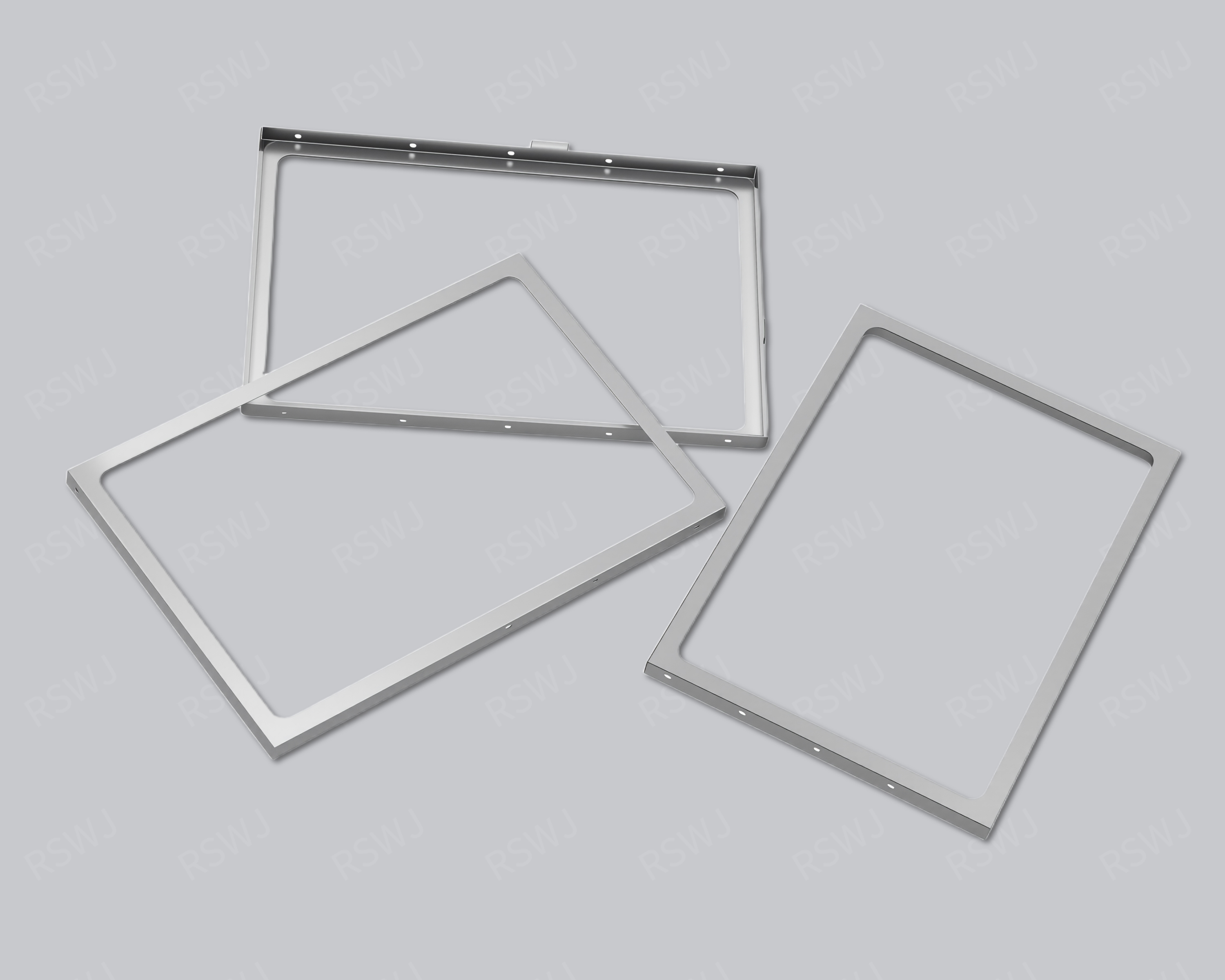
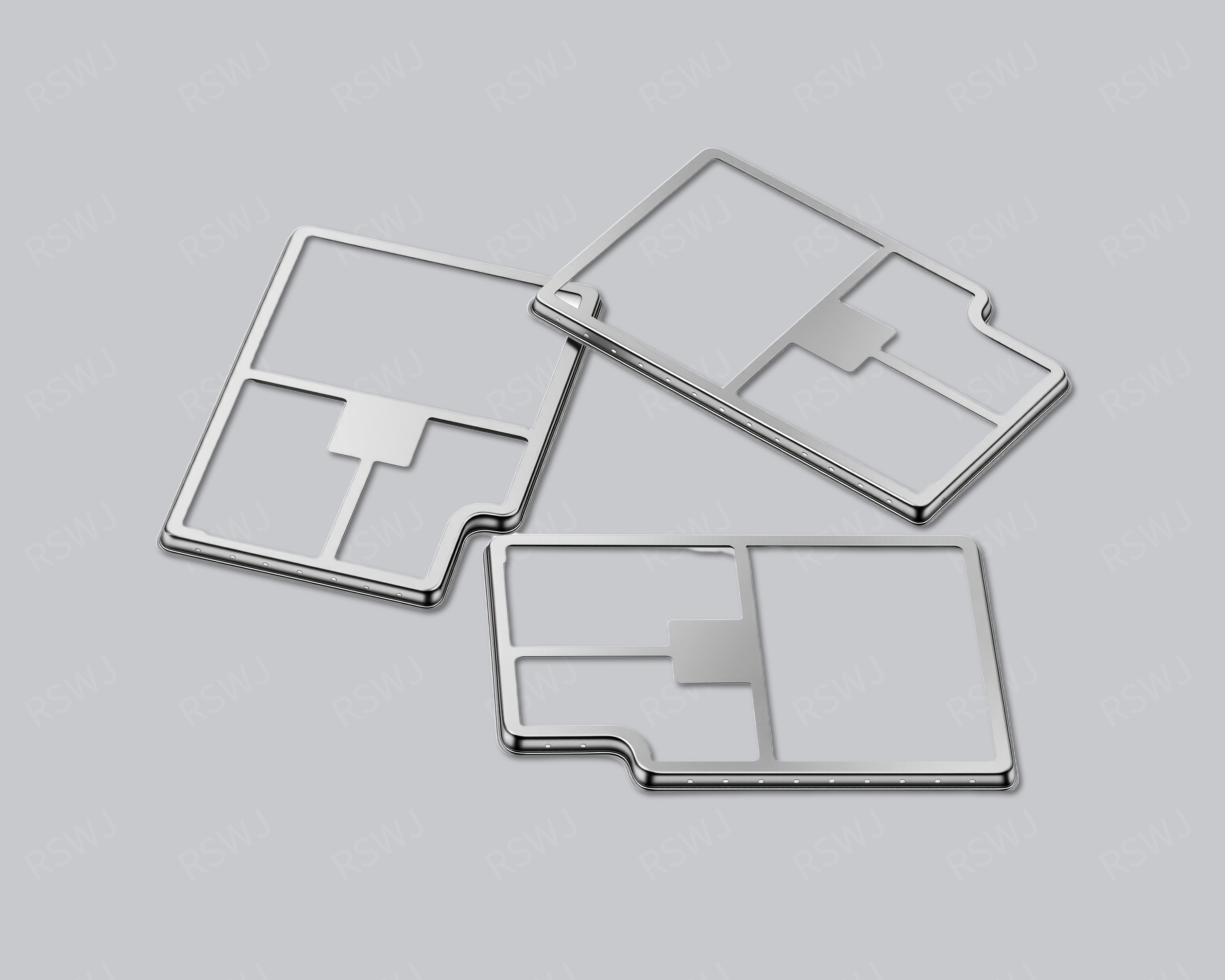
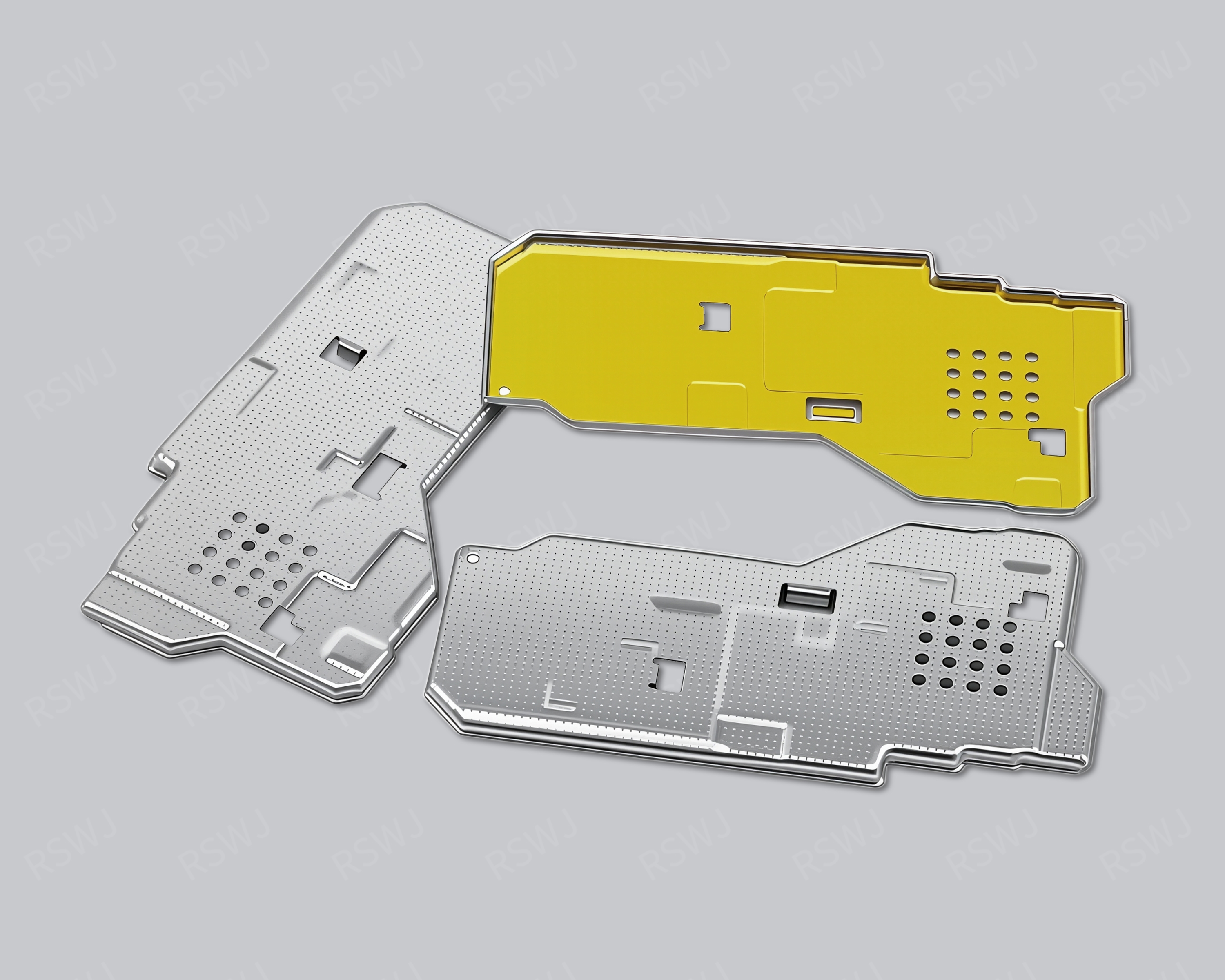
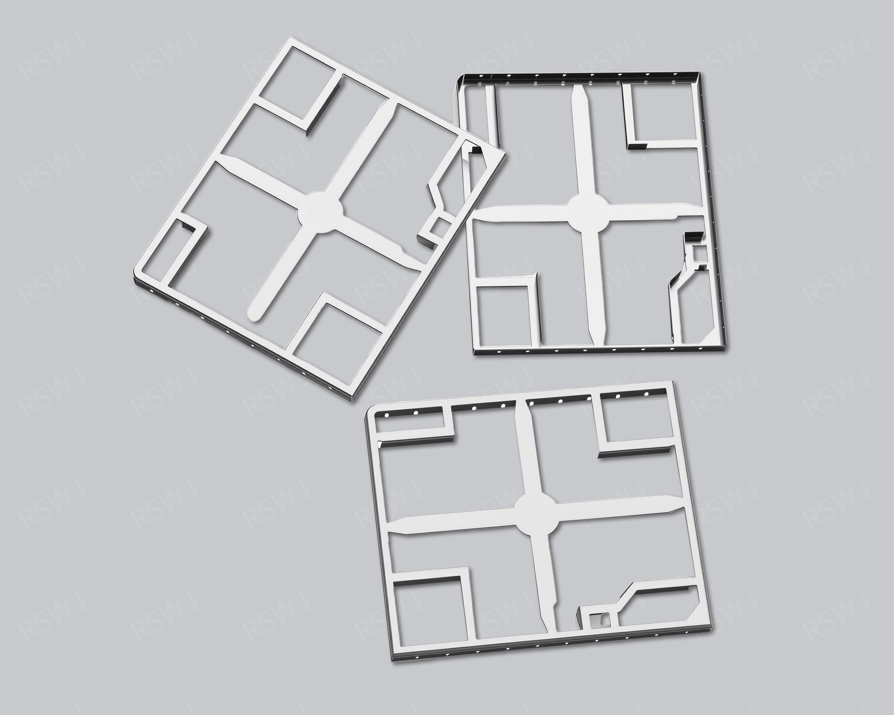
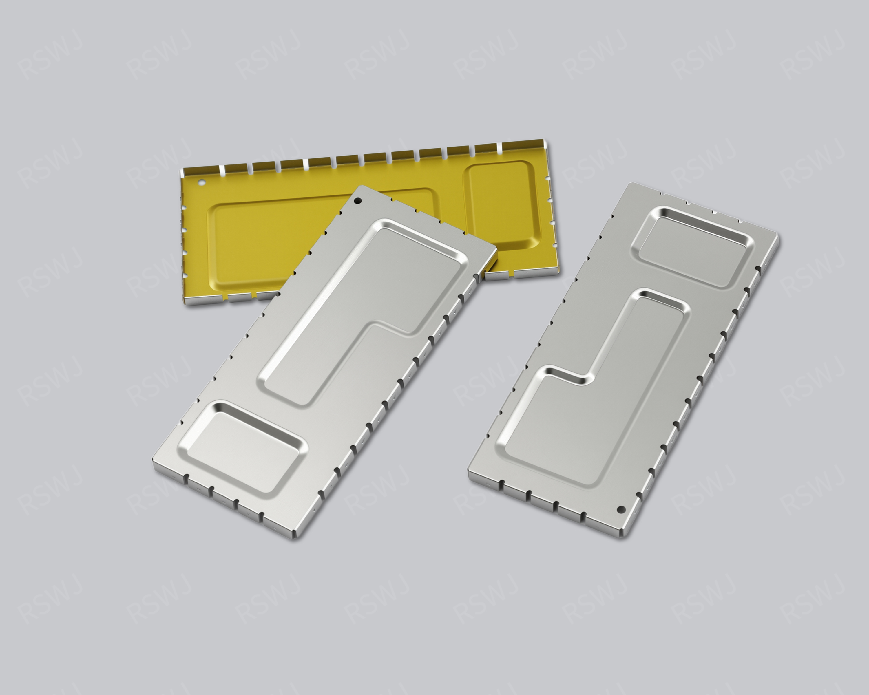
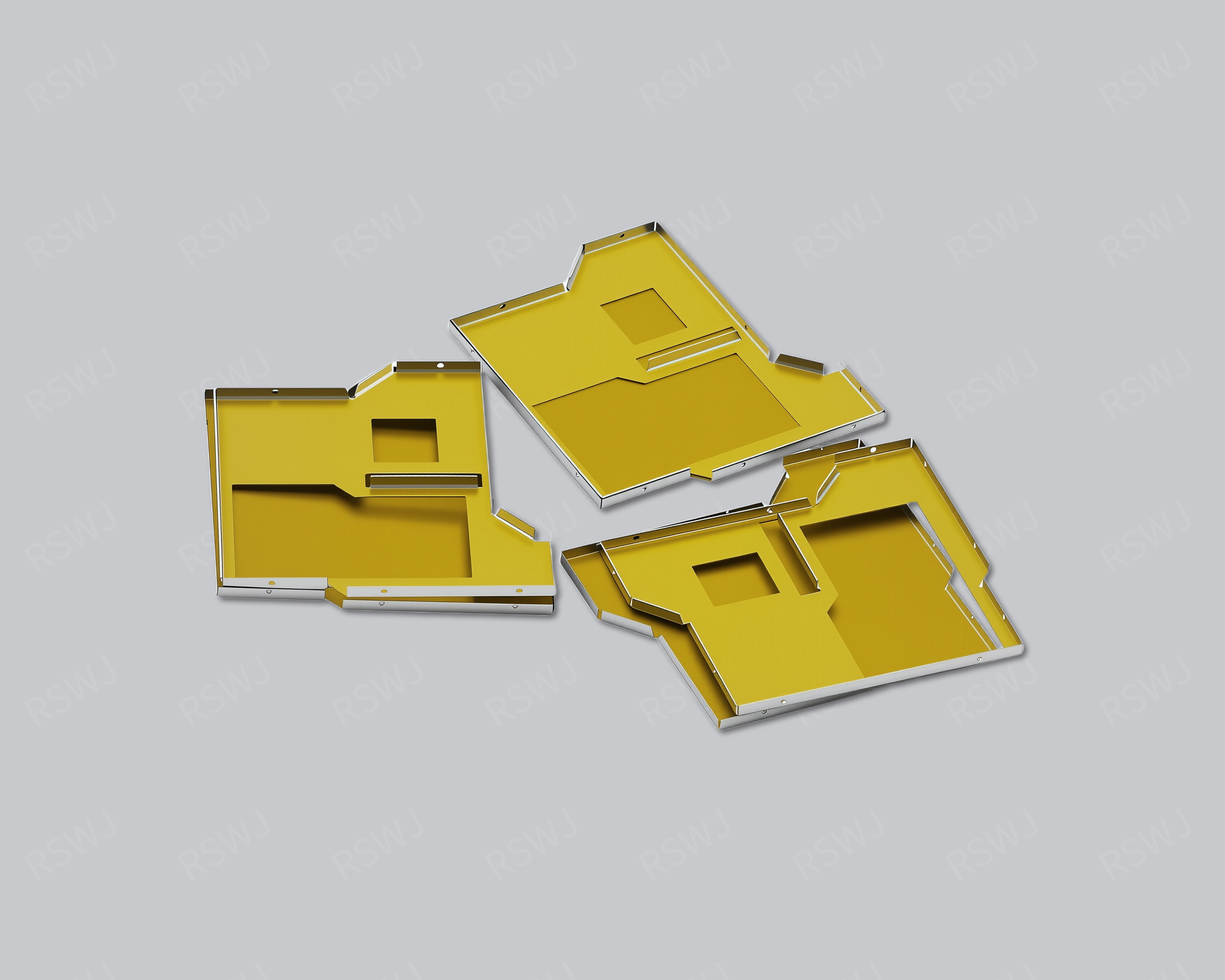
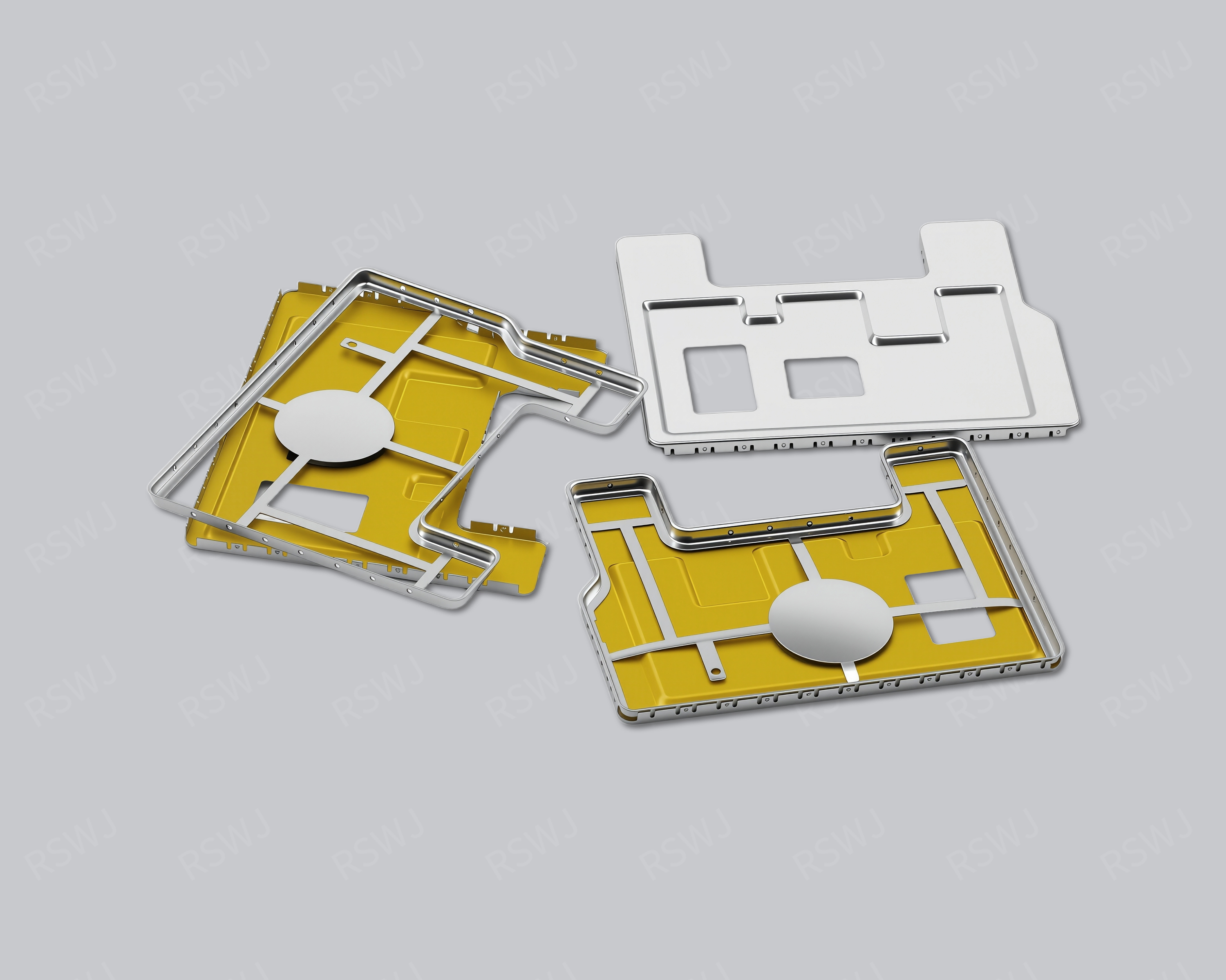
301 Stainless Steel EMI Shield
Specify the 301 grade and material condition before reviewing the shape, joining method and surface requirements.
View product
EMI SHIELDING PRODUCTS
Explore shield designs, materials and application examples. Find a starting point, then discuss fit, manufacturing and sample requirements with our team.
113 product entries
Specify the 301 grade and material condition before reviewing the shape, joining method and surface requirements.
View productStart with the 5G board layout, coverage boundary and connector clearances. Bring installation and system test conditions into the review.
View productFit the shield around the 5G module layout and component heights. Check the interface to the main board and the space needed for connections.
View productReview the ADAS module layout together with its installation interfaces. State the project environment and validation requirements with the drawing.
View productReview coverage around the AI module without treating cooling space or connector access as afterthoughts.
View productConfirm the aluminum grade and condition before reviewing forming, connections and the finish required at contact areas.
View productIdentify the part being covered and the antenna regions that must remain unobstructed, then review mounting and system validation.
View productDefine the automotive module's coverage and installation boundary alongside the environmental and validation requirements.
View productIdentify the circuit area to cover without obstructing the required RF and connection interfaces, then review installed grounding.
View productIdentify the vehicle-module application and installation interface, then agree on the environment and inspection conditions.
View productReview coverage and compartment boundaries alongside connectors, cooling interfaces and the module's installation requirements.
View productConfirm coverage, mounting and mating-part requirements from the drawing.
View productCheck the Bluetooth module boundary with antenna keepouts, interface openings and main-board fit shown together.
View productReview the PCB shielding boundary, solder pads and grounding points as part of the installed assembly and test plan.
View productDefine component coverage and partitions on the board, then check height, pad locations and the connection method.
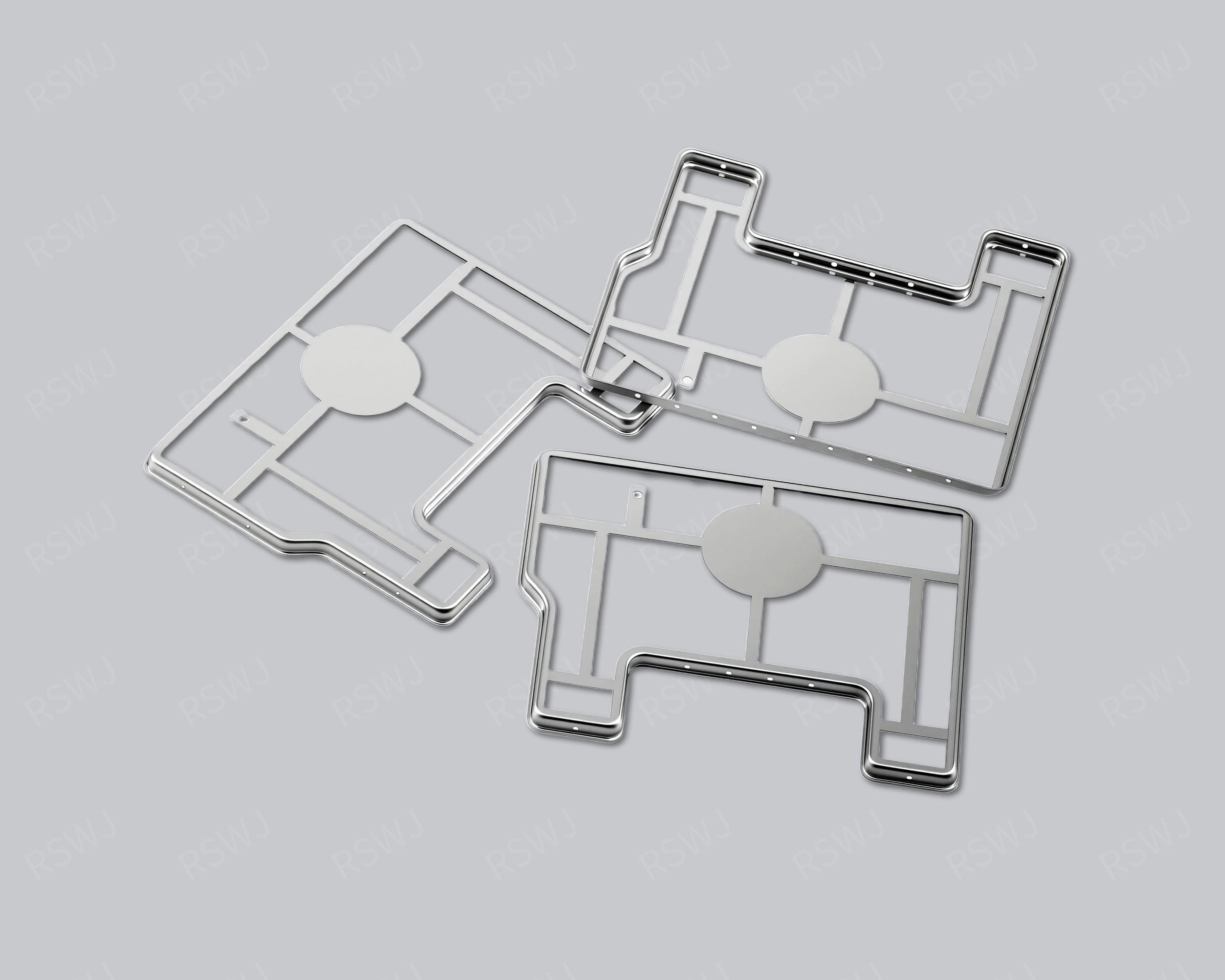
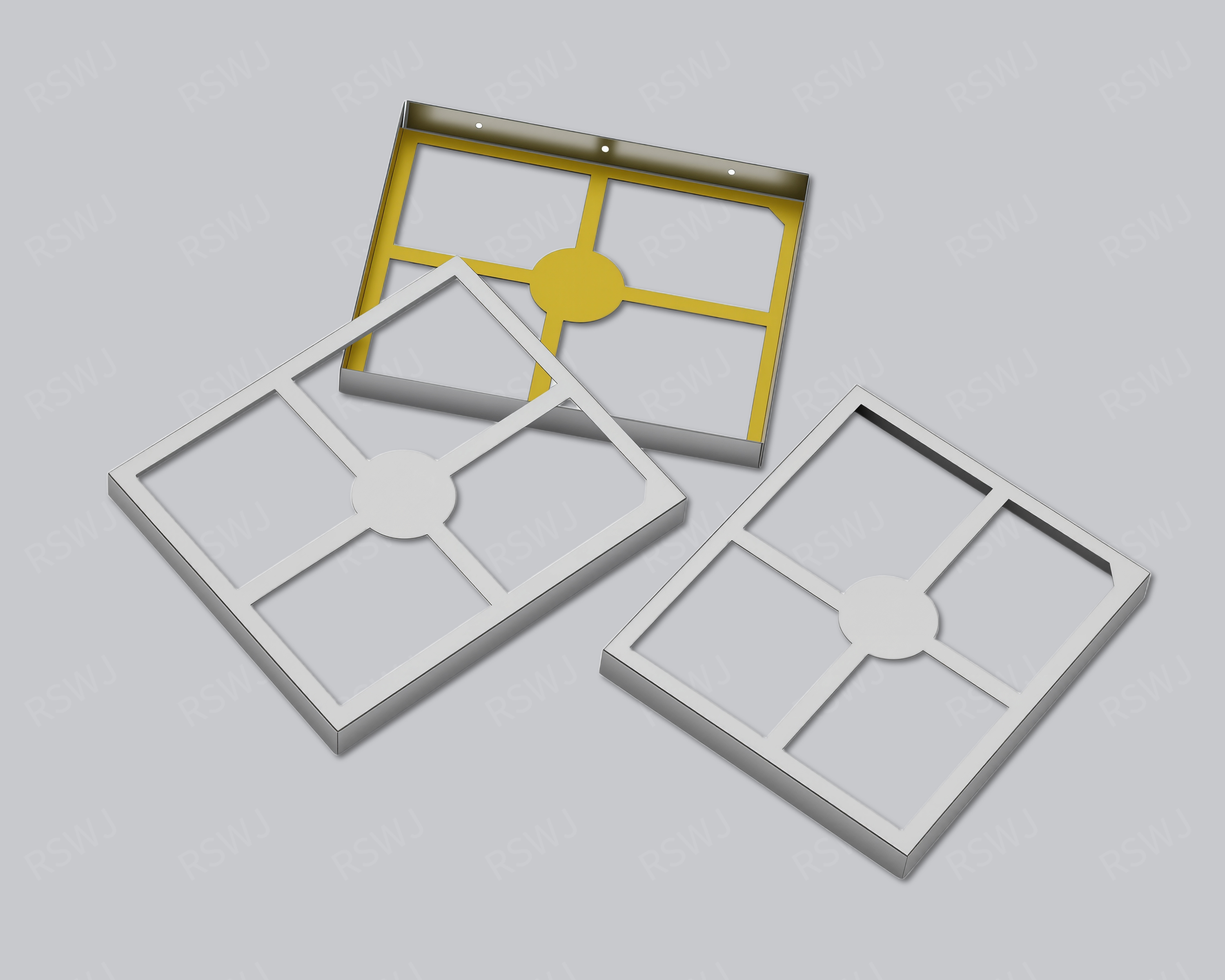
View productDefine the frame's inner and outer boundaries, then review the mating cover, solder locations and contact points.
View productUse the board and assembly drawings to define the part's coverage, clearances and installation requirements.
View productReview circuit coverage around the camera module without obstructing the lens, moving components or installed mounting space.
View productDefine coverage around the chip and neighboring parts, with pins, cooling clearances and board mounting shown on the drawing.
View productMark circuit coverage, partition boundaries and fixing locations before checking board height and connector clearance.
View productDefine the communications circuit coverage and connection openings before reviewing grounding and project test conditions.
View productReview the module outline, component partitions and interface positions against the main-board installation.
View productConfirm the requested copper-nickel grade rather than treating a broad material name as a complete specification.
View productDefine coverage around the CPU and nearby components while checking the space needed by cooling hardware and board connections.
View productBring the shielding objective, drawing revision and assembly limits into one review before selecting the manufacturing and sample approach.
View productReview the custom board revision, component keepouts and installation approach before agreeing on the sample scope.
View productBring the specified nickel silver grade, drawing geometry and joining requirements into the same custom-part review.
View productDefine the custom body outline, hole positions and mating dimensions before choosing a manufacturing route and sample scope.
View productDefine the RF operating conditions and connection openings alongside the assembly boundary, grounding method and test scope.
View productStart with the part's purpose, drawing revision and mating components, then agree on material, sample quantity and inspection scope.
View productReview coverage around the control or camera circuit, with lens, cable and connector clearances included in the installation layout.
View productReview body depth, corner geometry and material condition before agreeing on forming and hole-making requirements.
View productIdentify the display control or power circuit to cover, then check cable connections, installation space and service access.
View productReview the EV module's shielding objective and connection boundary with installation conditions and project tests defined separately.
View productIdentify the equipment circuit and part function before defining terminal clearances, mounting space and inspection requirements.
View productDefine the shielding objective and installed grounding arrangement, then select the material and validation method for the project.
View productDefine the coating scope, preserved contact areas and inspection conditions before specifying the paint or coating process.
View productDefine the circuit area to cover, then review the shield outline, mounting interface and project test requirements.
View productTurn quality requirements into measurable drawing and inspection criteria, covering fit, material and surface acceptance.
View productReview the clip against its mating surface and installed working space, including the fixing method and contact checks.
View productDefine the circuit coverage and installation method before narrowing the shield structure, material and validation requirements.
View productReview the fence's board position, edge dimensions and mating parts together with locating and grounding requirements.
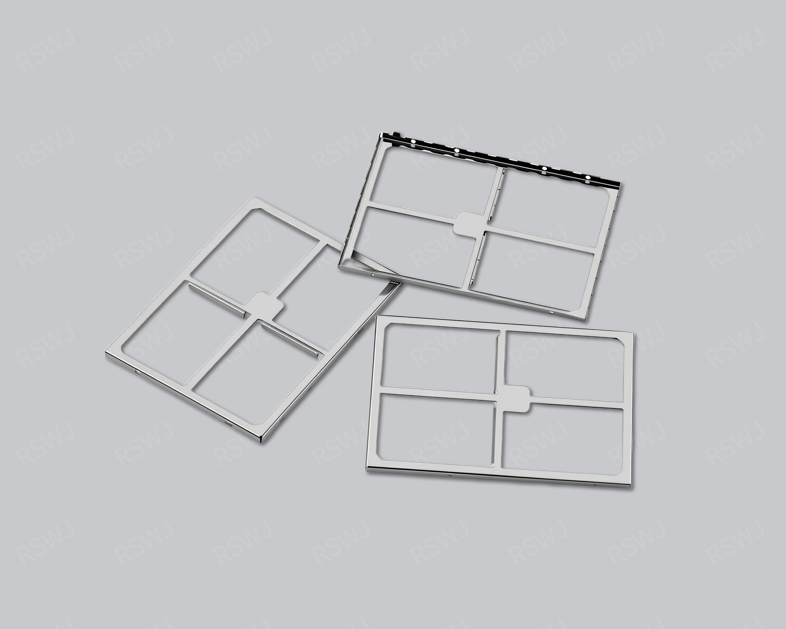
View productReview the frame's PCB boundary and its mating lid together, including locating features and electrical contact requirements.
View productMatch the lid to its frame or mounting interface. Review edge fit, removal space and the contact points as one assembly.
View productReview power-module coverage around terminals and cooling interfaces, with installation gaps and project test conditions stated.
View productCheck module and interface dimensions while preserving the space needed by fiber exits, cable routing and installation.
View productConfirm the complete frame-and-cover configuration rather than selecting from the frame outline alone.
View productMap the GPS-related circuit coverage alongside antenna and connection clearances before settling the shield outline.
View productCheck module dimensions, component height and connection openings against the main-board installation.
View productReview the graphics-card coverage area with the cooling assembly, connectors and mounting boundary shown together.
View productIdentify the vehicle device and module to cover, then define mounting interfaces, connections and project validation requirements.
View productReview control-board coverage alongside connectors and maintenance access, with the installation environment included in the drawing review.
View productReview circuit coverage alongside display and connection interfaces, including enclosure space and the fixing method.
View productIdentify the instrument circuit to cover and preserve the access needed by measurement interfaces, connections and maintenance.
View productSpecify the surfaces or gaps requiring insulation and distinguish them from areas that must provide contact or grounding.
View productReview laptop-board coverage within the space shared by cooling hardware, battery components and connections.
View productReview the shield's position inside the device alongside enclosure space, maintenance access and the project's inspection requirements.
View productIdentify the electronic module, assembly interfaces and project validation scope. Application naming does not establish device qualification.
View productPut the actual dimensions, component gaps and hole locations on the drawing so handling and inspection requirements can be reviewed.
View productDefine the phone project's circuit coverage, component keepouts and grounding interfaces before agreeing on the assembled test conditions.
View productDefine the covered and open areas on the motherboard, with component clearances, grounding points and interfaces shown together.
View productMark the motherboard area to cover and check component heights, interfaces and cooling clearances against the mounting boundary.
View productMap each compartment to the circuit layout, then review partition landing points, lid fit and access to the covered areas.
View productCheck board coverage around network interfaces and connectors, including installation and system validation requirements.
View productIdentify the vehicle module and its installation boundary, then state the project's environmental and verification requirements.
View productSpecify the nickel silver grade and condition before reviewing body forming, connections and contact surfaces.
View productSpecify the nickel silver grade, thickness and condition, then agree on joining and surface requirements for the drawing.
View productConfirm the material designation and supporting documentation, then review thickness, assembly and surface requirements.
View productDefine the base material, nickel coating and contact interfaces, with finished dimensions and inspection requirements stated.
View productReview the body outline, covered height and installation boundary, then decide whether the assembly needs access after installation.
View productReview the continuous body shape, corner geometry and openings. The drawing determines the forming approach rather than the name alone.
View productReview module coverage around optical ports and connections, with ventilation, installation and maintenance access shown on the drawing.
View productPlace the shield boundary, solder pads and grounding points on the PCB layout so height and assembly clearances can be reviewed together.
View productSpecify the requested permalloy grade and condition before reviewing forming, further treatment and the project's validation method.
View productReview the phone-board boundary against camera, connector and enclosure clearances, including installation and later access.
View productReview power-circuit coverage around terminals, cooling hardware and installation clearances.
View productState the critical dimensions and measurement method separately from the project's shielding objective and system test conditions.
View productDefine precision through tolerances, datums and acceptance criteria, with the mating assembly available for review.
View productConfirm which part is removable, how it is retained and how contact is maintained during the required access and reassembly.
View productCheck coverage, connection openings and grounding in the installed RF assembly, with the test method defined by the project.
View productState the RF project's coverage and operating conditions, then review openings, connections and the installed grounding arrangement.
View productIdentify the electronic module within the robot and review fixing points, connections and nearby moving hardware.
View productReview the router's circuit partitions alongside ports, cooling space and enclosure access.
View productReview server-board coverage alongside connectors, cooling hardware and the space required for installation and service.
View productStart with the device layout and shielding requirement. Define mounting interfaces and the checks needed before choosing a sample process.
View productIdentify the device module and review shield coverage alongside connections, enclosure space and installation conditions.
View productReview the lock's control or wireless module alongside connectors, moving hardware and maintenance access.
View productCheck the control or wireless module boundary with speaker hardware and connections included in the assembly review.
View productCheck smartphone-module coverage against camera, connector and height constraints before reviewing main-board mounting.
View productReview the watch PCB and covered circuits against battery, sensor and housing clearances, including small-part handling.
View productCheck pick-up geometry, pad contact and feeder packaging against the intended placement and reflow process.
View productReview the frame's pad layout, pick-up access and mating lid alongside the intended placement and reflow process.
View productReview the snap locations, mating part and installed contact areas before agreeing on retention and removal requirements.
View productReview circuit coverage alongside speaker hardware, connections and housing mounting, then define the system validation scope.
View productSpecify the stainless steel grade and condition, then review how forming, joining and surface requirements affect the assembly.
View productReview holes, bends and material thickness together so the stamping approach and critical inspection dimensions follow the drawing.
View productReview tablet-board coverage within the space shared by the housing, battery and connections.
View productIdentify the board or module inside the equipment, with enclosure, connector and maintenance interfaces available for review.
View productSpecify whether thin refers to wall thickness or installed height, then review component clearance and handling requirements.
View productSpecify the base material and tin coating separately, including soldering areas, contact surfaces and inspection requirements.
View productConfirm the tinplate material and coating condition, then review thickness, forming and connections for the board-level design.
View productDefine coverage around the transformer and nearby parts while preserving terminal clearances and installation space.
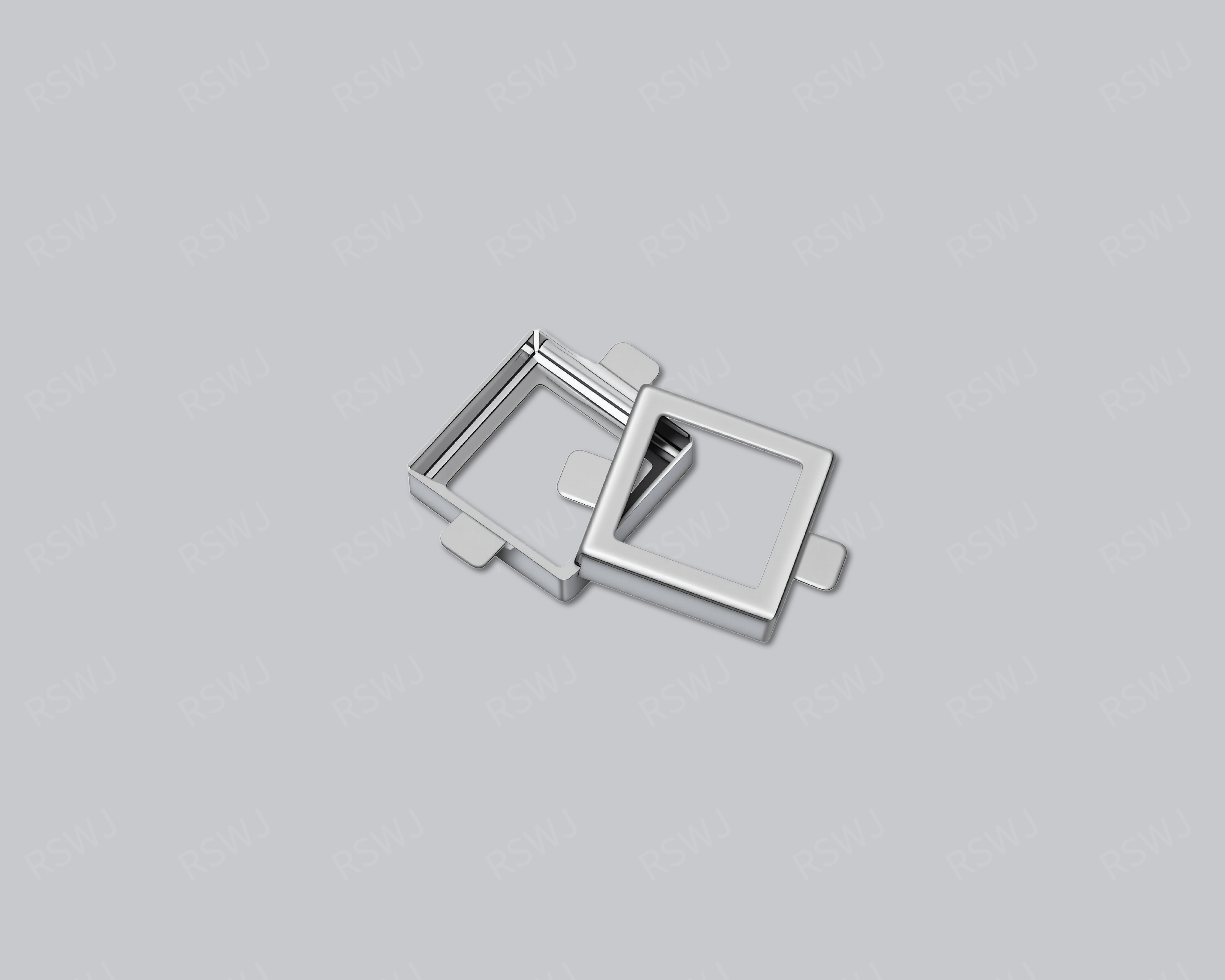
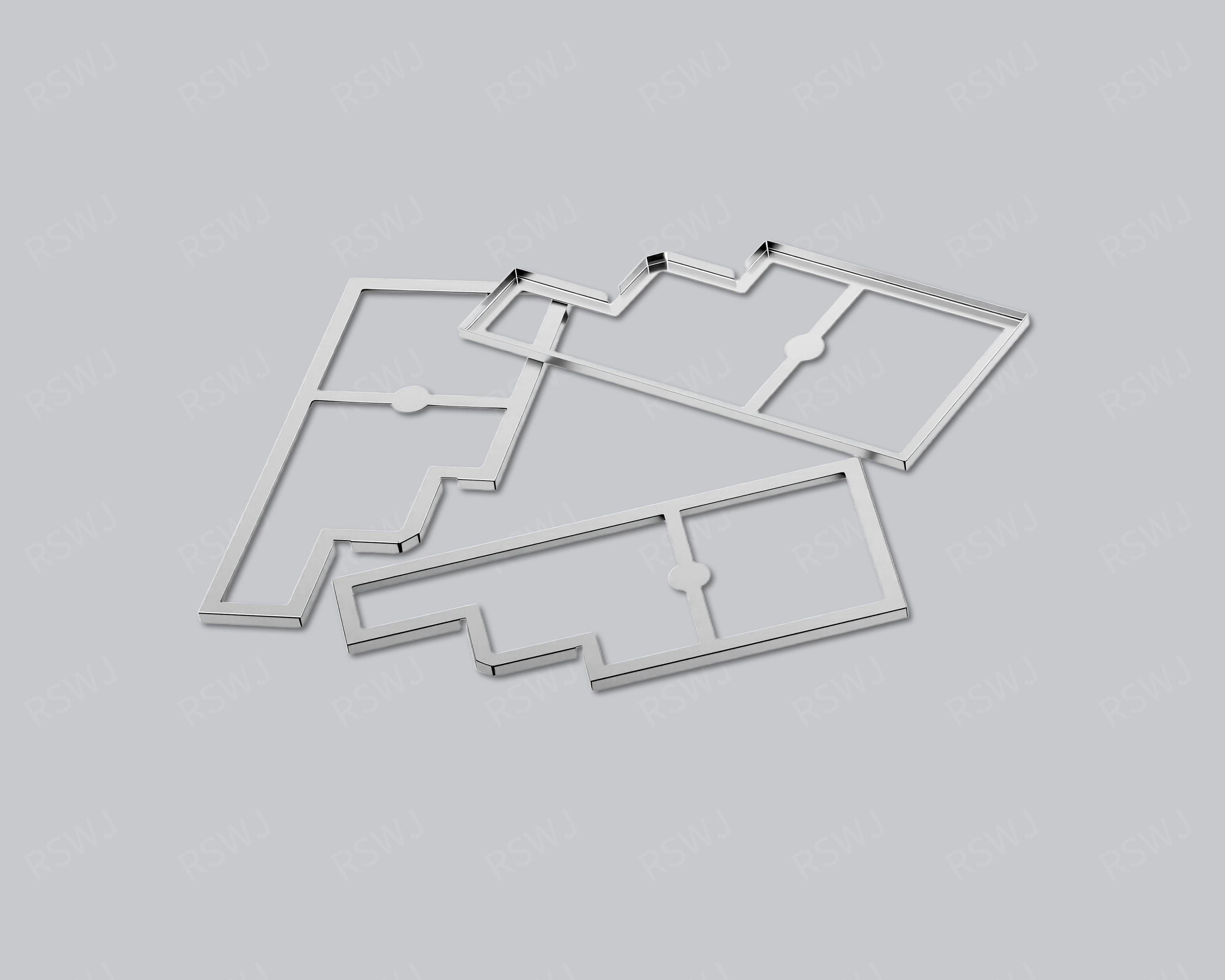
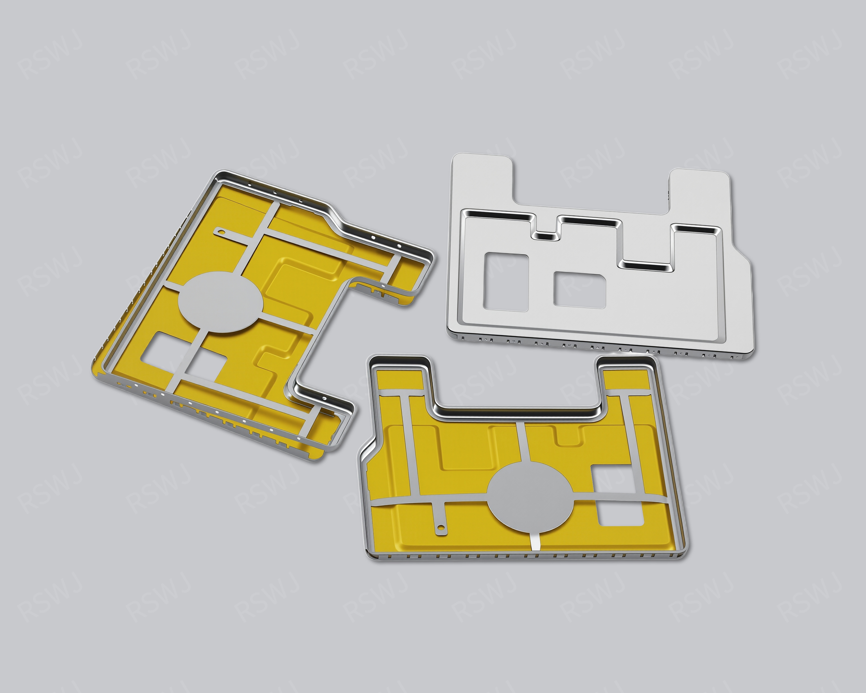
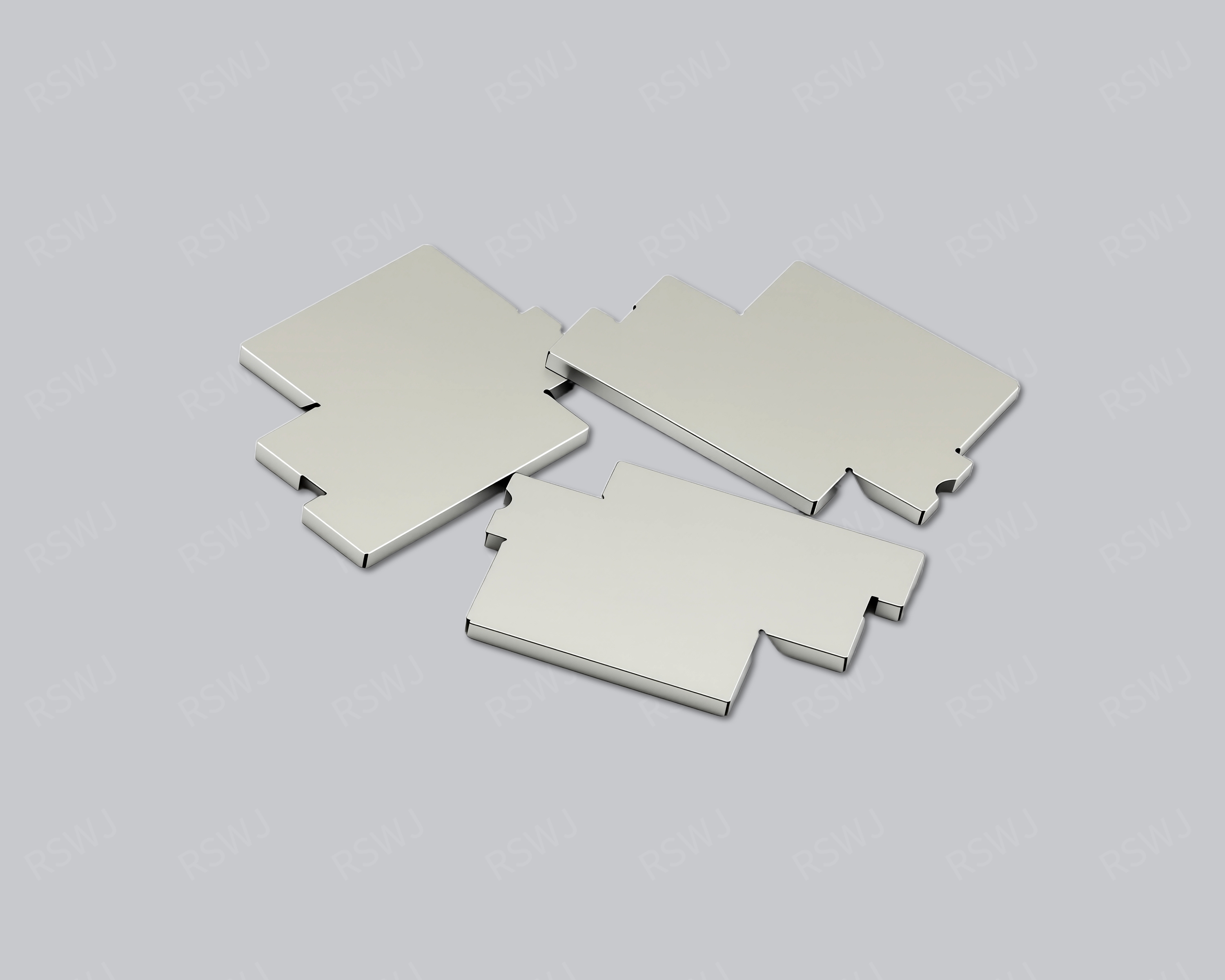
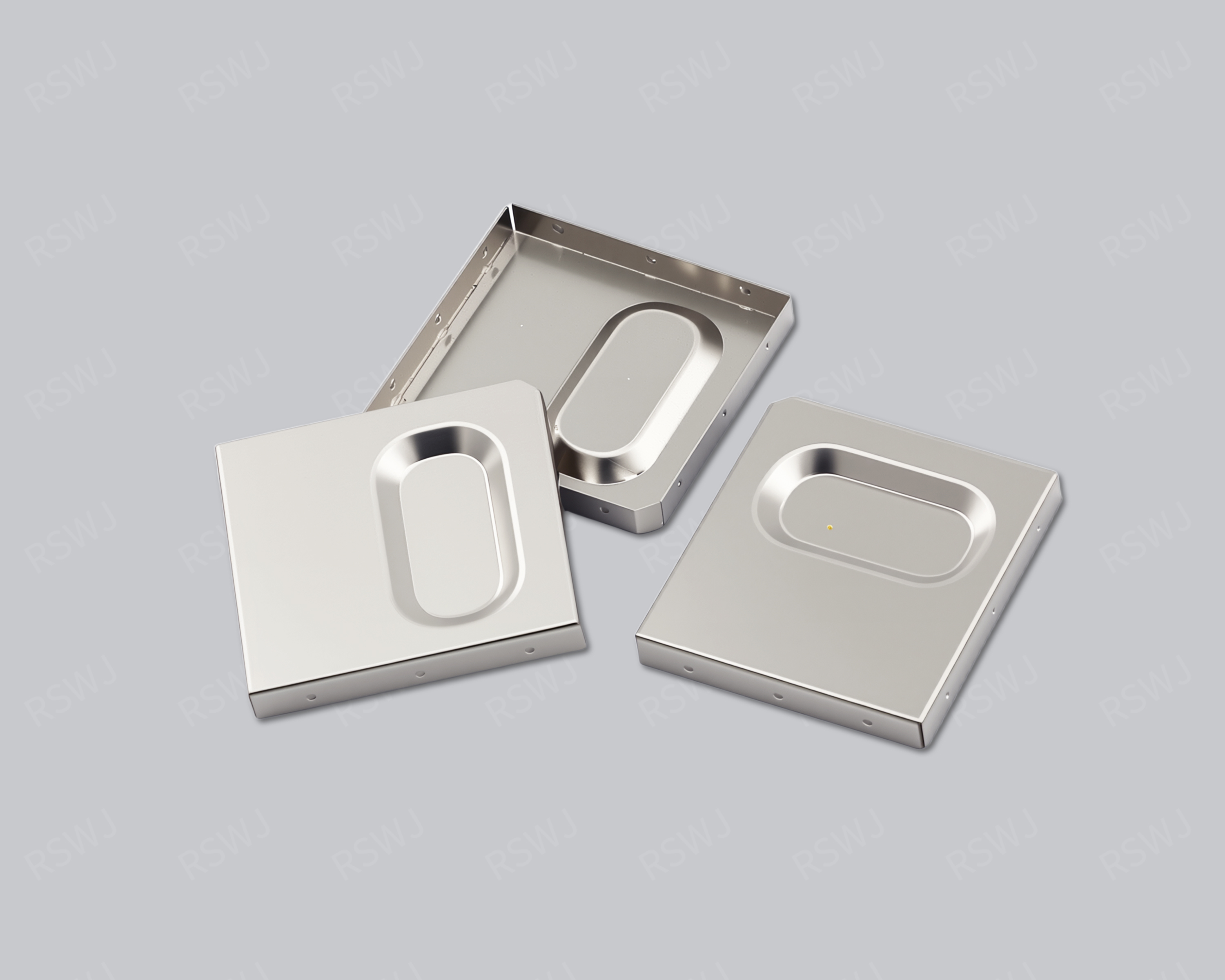
View productBring both part drawings and the assembly view into the review. Confirm contact fit, access needs and the removal method together.
View productReview frame-to-lid fit, contact areas and the space needed to remove the lid as part of the complete PCB assembly.
View productReview the separate shield parts as one assembly, including mating dimensions, assembly order and service access.
View productReview the earbud PCB boundary within the space shared by the battery, housing and connections.
View productIdentify the module to cover and review shield space alongside optical hardware, connections and board mounting.
View productReview the wearable PCB, battery and housing as a single space constraint before defining the shield's mounting interface.
View productCheck the WiFi module layout, antenna keepouts and connection openings against the shield height and main-board interface.
View productCheck the wireless module layout against antenna keepouts, connection positions and main-board installation space.
View productReview router-board partitions alongside antenna, port and cooling interfaces before defining the shield's enclosure fit.
View productDefine the target circuit coverage and the openings that remain available, with signal test conditions based on the installed system.
View productClarify whether zinc describes the base material or another requirement, then review forming, finish and assembly interfaces.
View productTry a different term or clear the filters to browse the full collection.
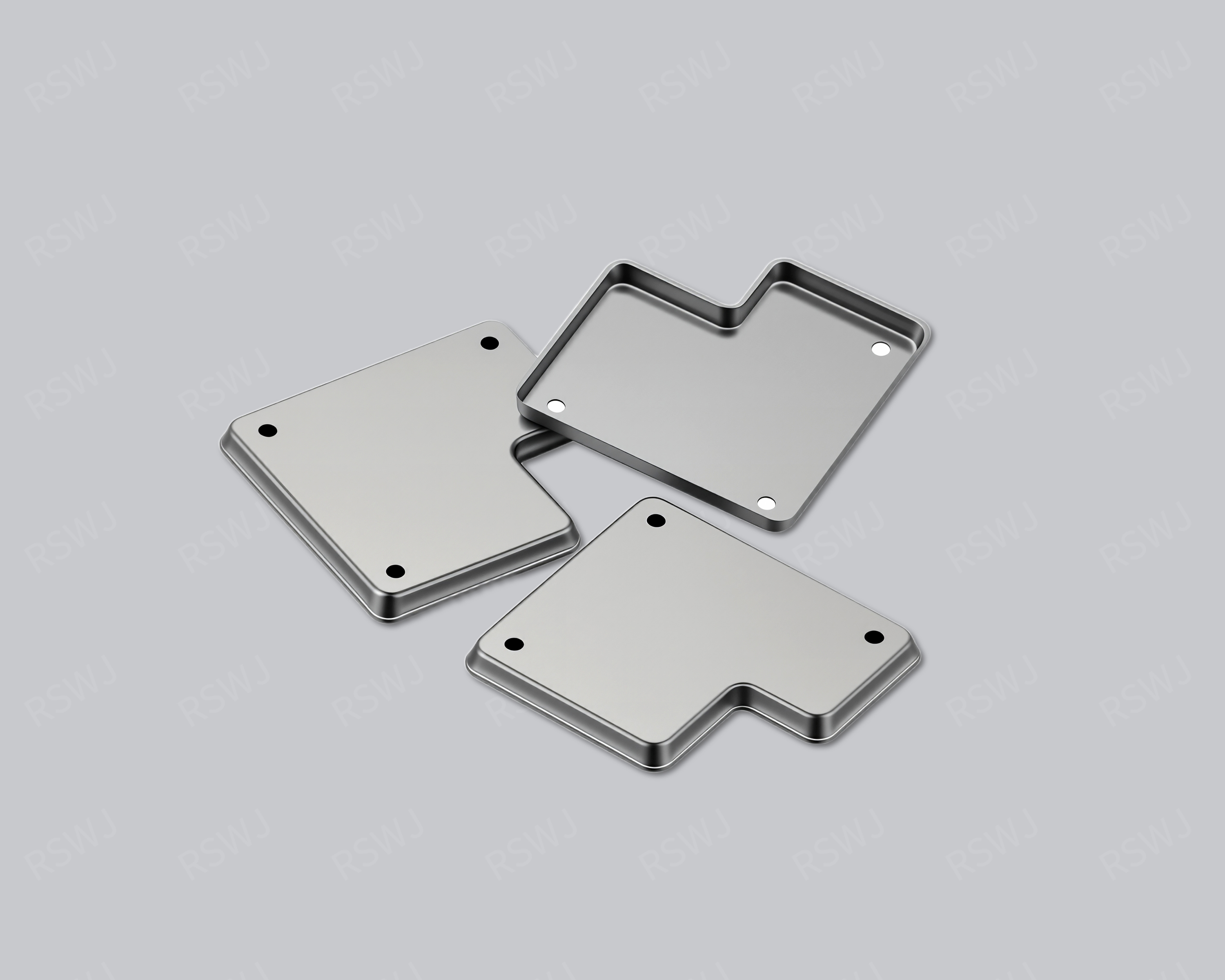
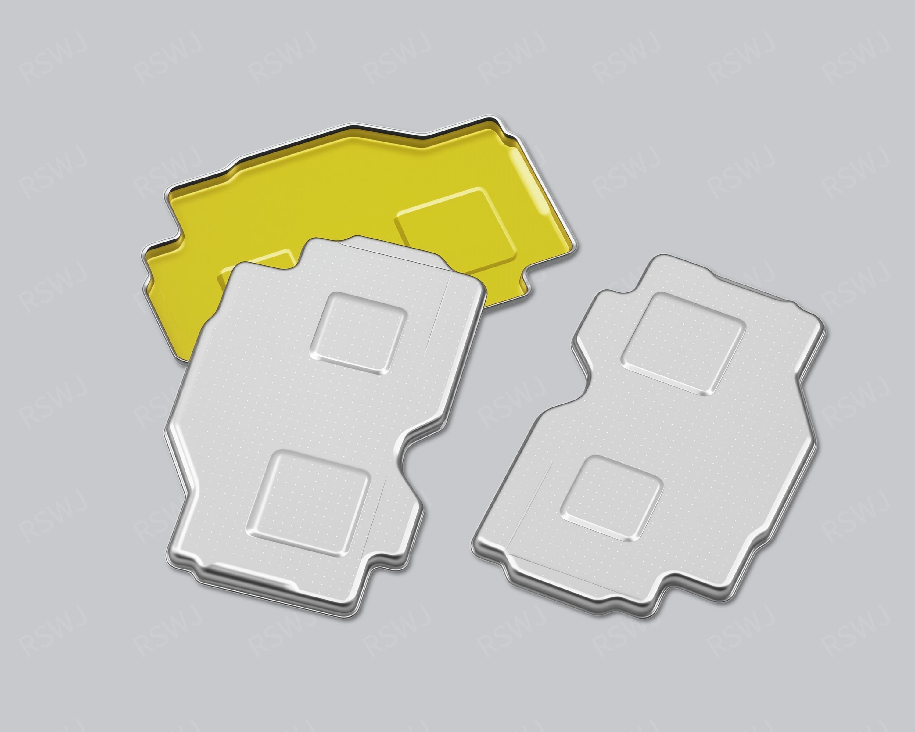
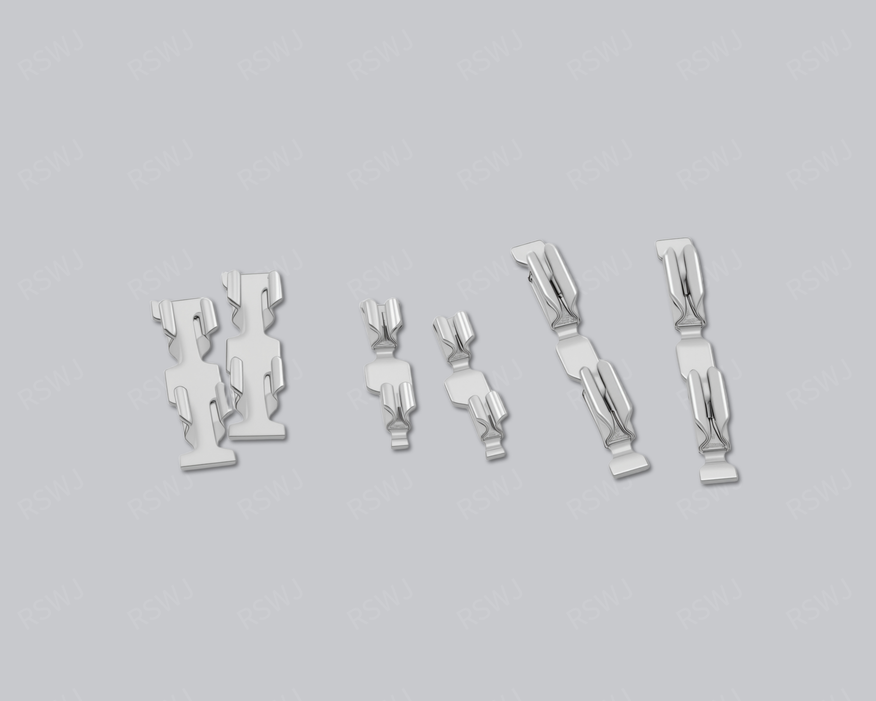
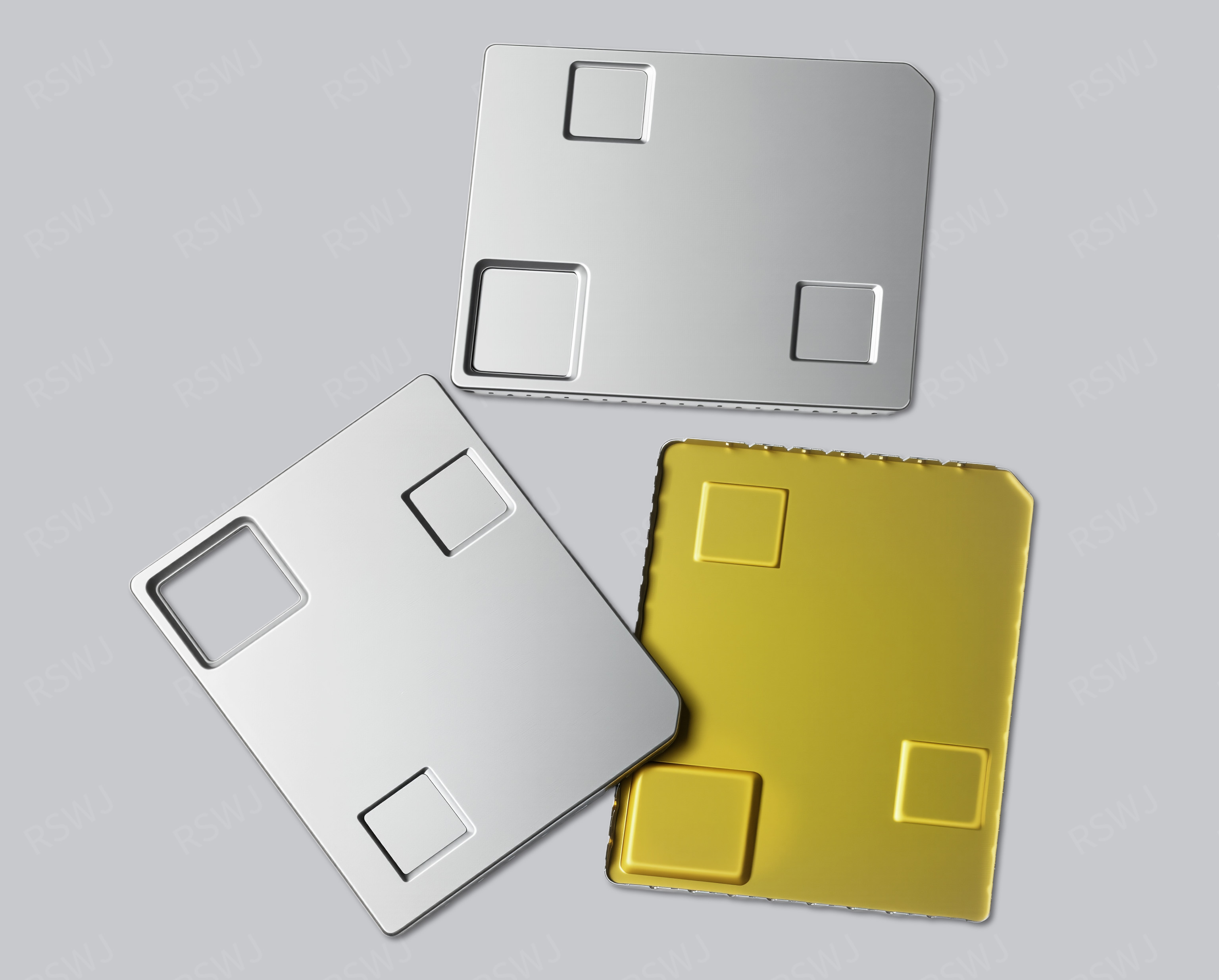
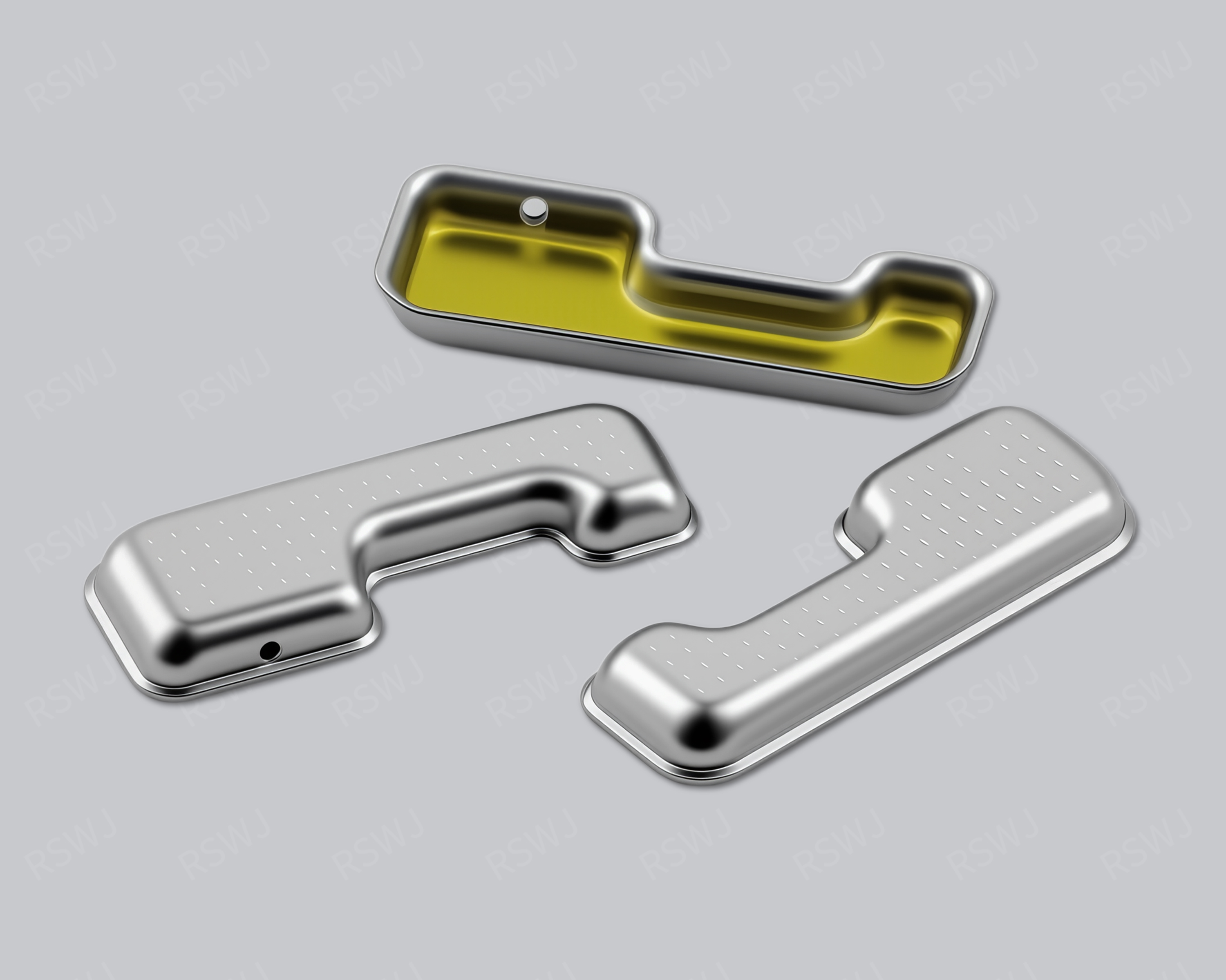
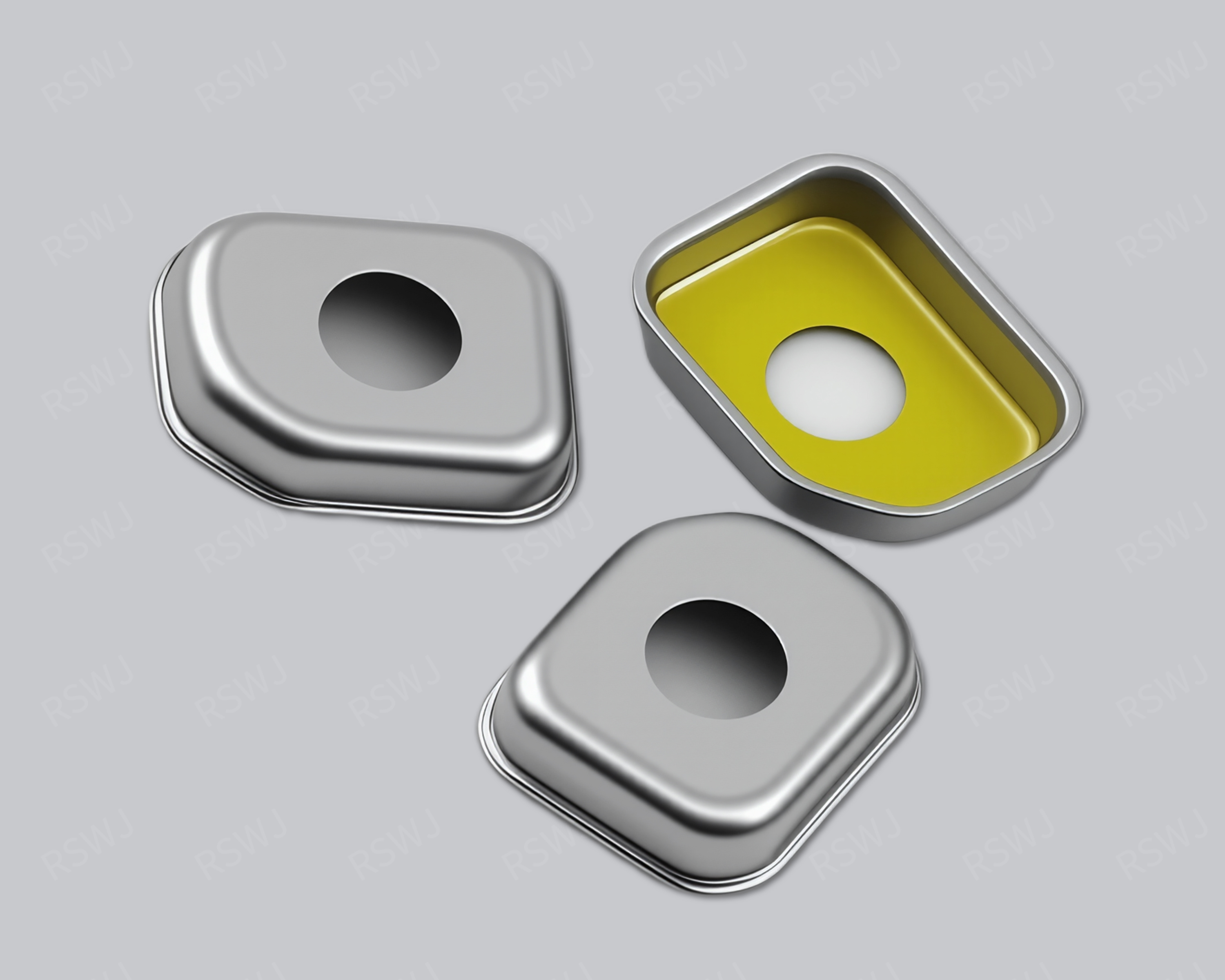
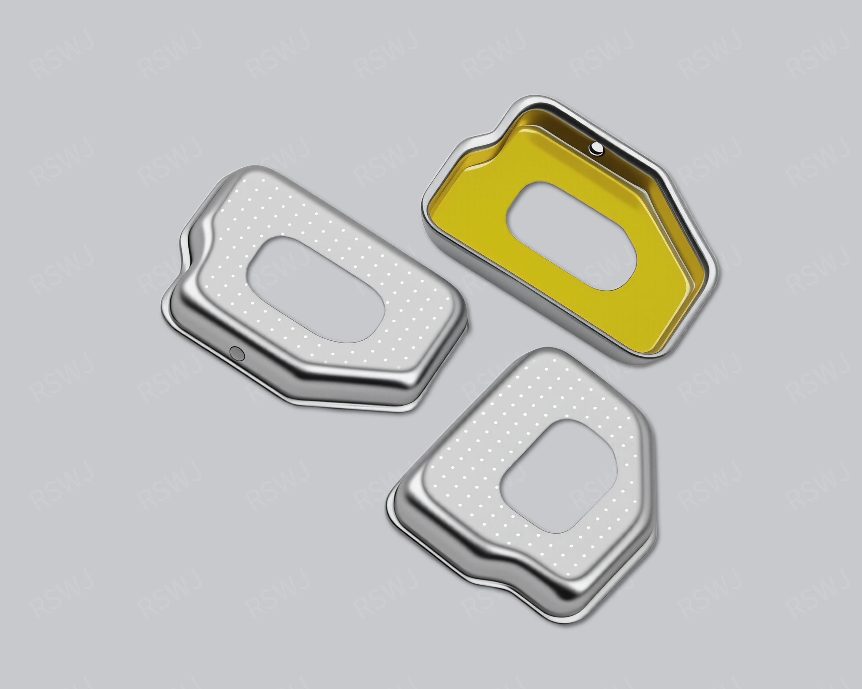
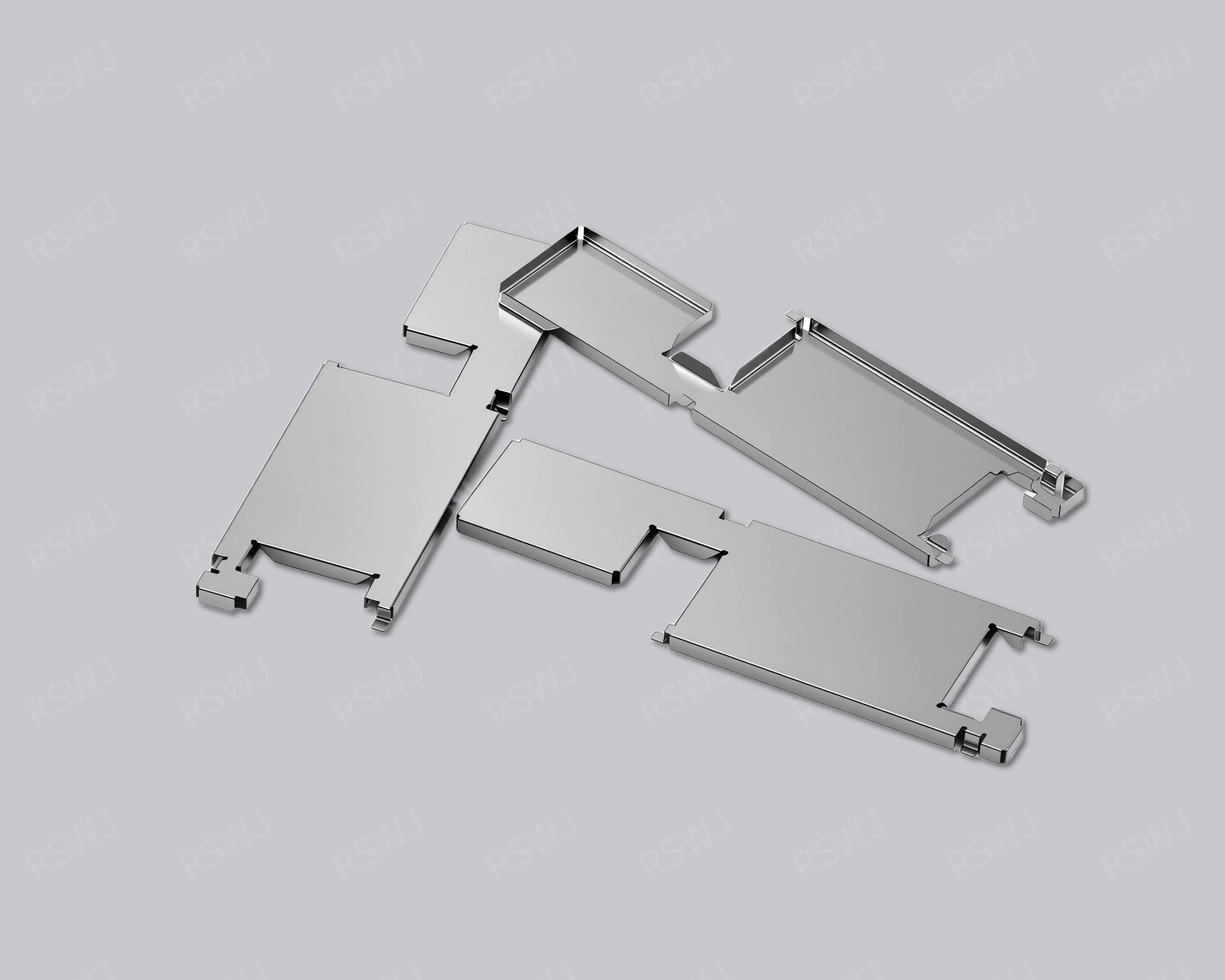
Images illustrate part geometry. Dimensions, material, finish and performance requirements are agreed through drawings, approved samples and project-specific validation.