
Start with the circuit regions that need coverage
A multi-cavity shield frame divides a covered PCB area into compartments. Its layout should explain which circuit belongs in each compartment, where the dividing walls meet the board and how connections cross those boundaries. Counting cavities does not answer those questions or establish shielding performance.
Begin with the current PCB placement and routing information. Mark the circuit groups being considered for separate coverage, the reason for each boundary and the parts that must remain outside it. A sensitive input circuit, a control section and a power circuit may raise different review questions. Their names alone do not determine the wall positions.
Use the multi-cavity shielding overview for the broader structure discussion. This guide focuses on the information needed to turn proposed circuit regions into a frame layout that can be reviewed against the board.
Build one layout package for the board and frame
Give each proposed compartment an identifier and connect it to component reference designators. Include the board outline, mounting holes, connectors, component outlines and relevant height information. Keep these views under the same PCB revision. A schematic block diagram explains function; the placement drawing explains whether a wall can occupy the proposed route.
Functional placement and signal routing also matter below the shield. High-speed layout guidance emphasizes reviewing connections between circuit groups together with their return-current paths. A physical partition on top of the board does not replace that electrical layout review.
Supply the relevant layer information where a connection crosses a proposed boundary. Identify its reference plane and any features that affect the return path. Distinguish the proposed shield attachment areas from unrelated copper. The PCB designer should explain the electrical role of those areas rather than leaving the shield supplier to infer it from a screenshot.
Circuit-region labels are not instructions to split a ground plane. Blindly introducing ground gaps can increase return-path inductance, and a trace crossing a gap can force its return current onto a longer route. Keep grounding and routing decisions tied to the circuit requirements and applicable component guidance.
An illustrative partition map
The map below is fictional and shows discussion relationships only. It is not a customer layout, is not to scale and contains no project dimensions. Table cells do not specify copper, wall thickness, mounting pads or openings.
| Left covered region | Proposed boundary corridor | Right covered region |
|---|---|---|
| Cavity A Sensitive circuit group | Wall W1 Connection X1 between A and B requires review | Cavity B Control circuit group |
| Cavity A continues No divider proposed here | W1 and W2 junction Attachment and contact to define | Wall W2 Proposed boundary between B and C |
| Cavity A continues Component heights to supply | W1 continues Board landing route to define | Cavity C Power circuit group |
Read W1 as the proposed divider between A and the right-hand regions; W2 divides B from C. X1 identifies a connection needing review, without prescribing its layer route or a wall cutout. To use this method on a real board, replace the labels with circuit identifiers and define every boundary from controlled PCB data.
Review where every wall lands
An internal wall needs a defined interface at the board. Show the intended wall route, attachment features and any specified electrical contact areas together. Then compare them with pads, vias, traces, component bodies and assembly keep-outs. A line drawn between two groups does not show whether the frame can actually be installed there.
Inspect wall junctions as well as straight sections. Where an internal divider meets another divider or the outer frame, ask how the geometry is formed, how it seats and which interfaces require inspection. If a proposed landing route conflicts with a component, record the conflict before choosing whether to move the component, revise the wall or change the compartment arrangement.
Review vertical space separately for each cavity. Include component bodies, leads and any neighboring structure that extends into the covered region. Show the board datum, installed frame position, wall height and lid relationship in useful sections. External shield height alone cannot establish the space available above a component.
Specify material and finish requirements in the drawing package, including areas intended for attachment or contact. Leave unresolved choices marked for discussion. The review should produce defined interfaces and inspection criteria, rather than treating a material name as proof of fit.
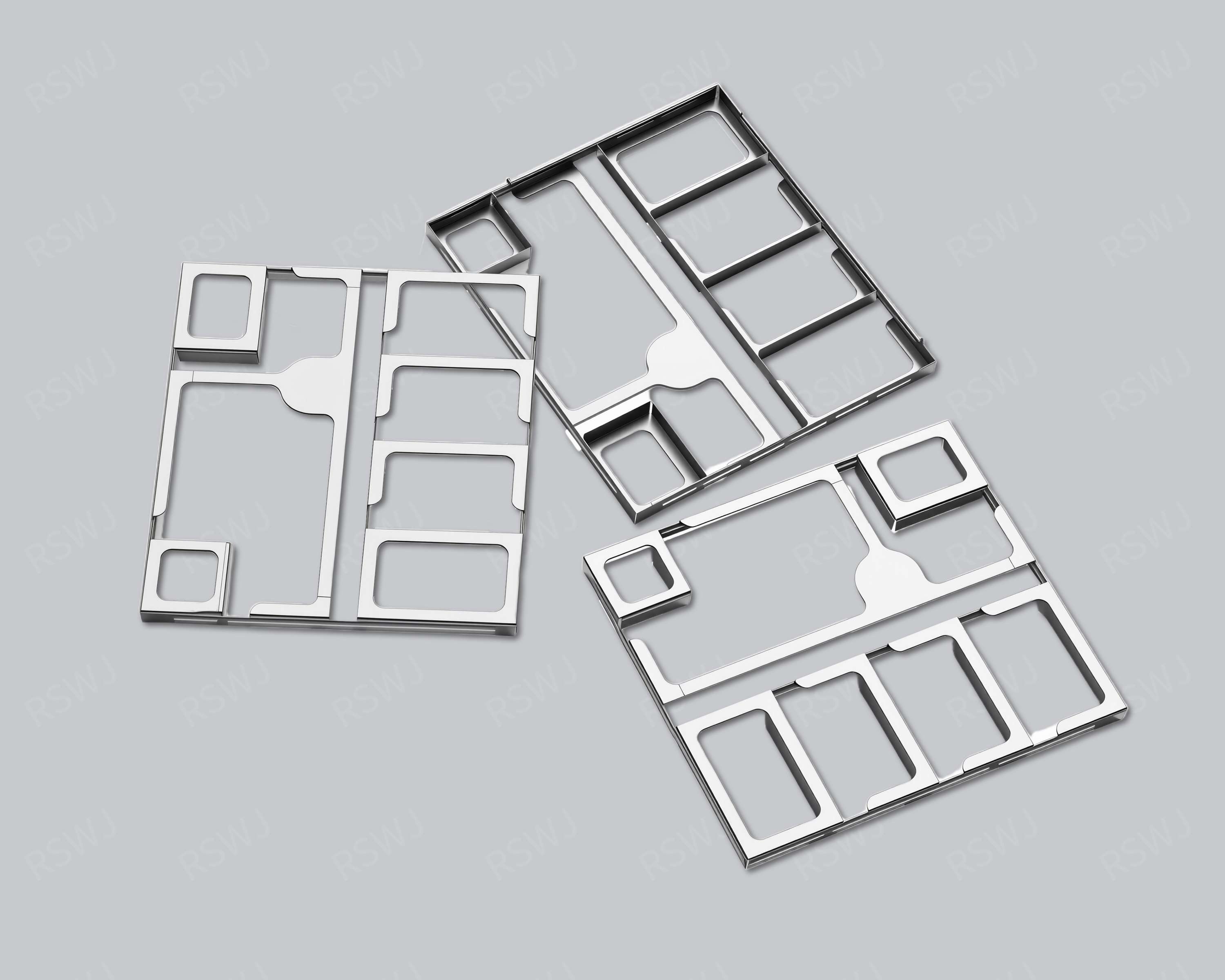
Product photograph from the Multi-Cavity EMI Shield product page. Use it to discuss the general structure; partition locations, dimensions, materials and performance for a project require the corresponding drawings and validation.
Give every crossing and opening a purpose
List the connections that move between compartments or leave the covered area. For each one, record the affected circuits, physical route, layer information and any component that occupies the boundary. A buried trace crossing and a connector body passing through a wall present different mechanical questions; do not describe both simply as an opening.
For a physical opening, specify what it must clear and what must remain covered. A cable, connector, locating feature or handling feature should have its own explanation. Mark the opening against the wall, adjacent parts and lid geometry. If its position remains undecided, identify the information needed to choose it.
Check whether a crossing changes a proposed landing or contact area. Discuss the resulting geometry with the PCB and shield designers together. Filtering, routing or grounding changes belong in the electrical design review, with their own acceptance criteria. Adding a wall cutout by itself does not establish that the connection is adequately controlled.
Assign a change record to each important opening. If a connector moves, revisit the boundary, mounting interface and test plan together. This prevents a small board-layout revision from leaving the shield drawing aligned with an older connection route.
Choose the lid arrangement around the compartments
Multi-compartment shielding can be built in a frame-and-cover arrangement. Decide whether the project needs one cover across the frame or separately handled covers over selected regions. Treat those as alternatives to review with the supplier, rather than assuming that any frame can accept either approach.
With a common cover, identify how its underside relates to every partition where contact or another interface is required. Check the complete seating arrangement, including internal walls and the outer boundary. If one cavity contains a taller component or a thermal interface, include that difference in the assembly section instead of assuming all compartments share the same usable height.
With separate covers, identify the boundary and mating interface for each cover. Review any shared wall, adjacent cover edges and the installation sequence. Ask whether fitting one cover affects another and how each combination will be identified during sample evaluation. Separate access is a requirement to develop, not evidence of better isolation.
Also define when the frame and covers enter the assembly process. Identify inspections that occur before closure and areas that must remain reachable. Keep placement, attachment and inspection requirements in the process review. The custom shielding design review can help structure the manufacturing discussion.
Validate the partitioned assembly with project samples
Agree the sample tasks before ordering parts. An initial dimensional check should assess the frame against the specified drawing. An assembly trial should then check the wall landing routes, component space, openings and lid arrangement against representative PCB and enclosure parts. Record which revisions and configurations were used.
For the illustrative map, the trial questions would include whether W1 occupies its approved landing route, whether the W1/W2 junction seats as intended and whether X1 can be accommodated without an unplanned geometry change. A common cover would need checks across the specified internal interfaces; separate covers would need the agreed individual and combined assembly checks.
Keep mechanical findings distinguishable from electrical results. Seating, clearance and access checks do not demonstrate attenuation between circuits. The project team should define the relevant operating states, measurements, fixtures and acceptance criteria for its EMI or RF validation. Cavity count alone cannot supply those criteria.
If the sample reveals interference, identify the responsible board or shield feature before revising the layout. Record the proposed change, the affected compartment and the checks to repeat. Moving an internal wall may alter several neighboring interfaces, so update the shared layout package before approving another sample.
Send an RFQ that preserves the layout decisions
A useful quotation package connects the proposed compartments to the actual board, with unresolved decisions clearly marked. Include:
- The PCB revision, component placement, relevant routing and height information.
- Compartment identifiers, coverage boundaries and the reason for each partition.
- Wall landing routes, attachment areas, contact requirements and assembly keep-outs.
- Cross-boundary connections and openings, with their purposes and mating parts.
- The proposed cover arrangement, assembly sequence and sample inspection tasks.
- Specified material and finish requirements, sample quantities, expected batch quantities and project dates.
Ruishuo's samples are charged. Standard samples are 3–5 days, expedited sampling is 48 hours, and tooling with sample production is 7–10 days. Confirm the suitable route and scope for the design; these are sample-stage timings. Volume production and delivery are arranged separately for the project.
Use the project inquiry page to describe the partition review. The website form records selected drawing file names. Email the actual drawing files separately to chinarswj@shieldingcover.com, including the revision used for the compartment map.
Frequently asked questions
Should each functional block have its own cavity?
Use the circuit objectives and actual layout to propose boundaries. Check connections, landing space and component clearances before deciding the compartment count. More compartments introduce more interfaces to review and do not establish better system performance.
Can a component or trace cross a partition?
Identify the actual crossing first. A trace on a board layer needs routing and return-path review; a component or connector at a wall also needs a defined mechanical relationship. Provide the relevant views and discuss the boundary before treating the crossing as resolved.
What needs approval before the frame layout is released?
Approve the shared PCB and shield revisions, wall interfaces, openings and cover arrangement. Resolve sample-fit findings and identify any outstanding electrical validation. Release drawings that describe the accepted configuration, with the inspection and production requirements agreed for that revision.